Field emission display device

A display element and field emission technology, which is applied in the direction of electrical components, image/graphic display tubes, semiconductor devices, etc., can solve the problem of high power consumption of components, achieve the effects of reducing emission voltage, facilitating tip discharge, and improving emission accuracy

Inactive Publication Date: 2004-01-14
HONG FU JIN PRECISION IND (SHENZHEN) CO LTD +1
View PDF0 Cites 5 Cited by
  • Summary
  • Abstract
  • Description
  • Claims
  • Application Information

AI Technical Summary

Problems solved by technology

[0007] However, a typical field emission display element needs to provide a high voltage between the cathode and the anode, which is usually higher than 1000 volts, which makes the power consumption of the element extremely large

Method used


Image

  • Field emission display device
  • Field emission display device
  • Field emission display device

Examples


Embodiment Construction

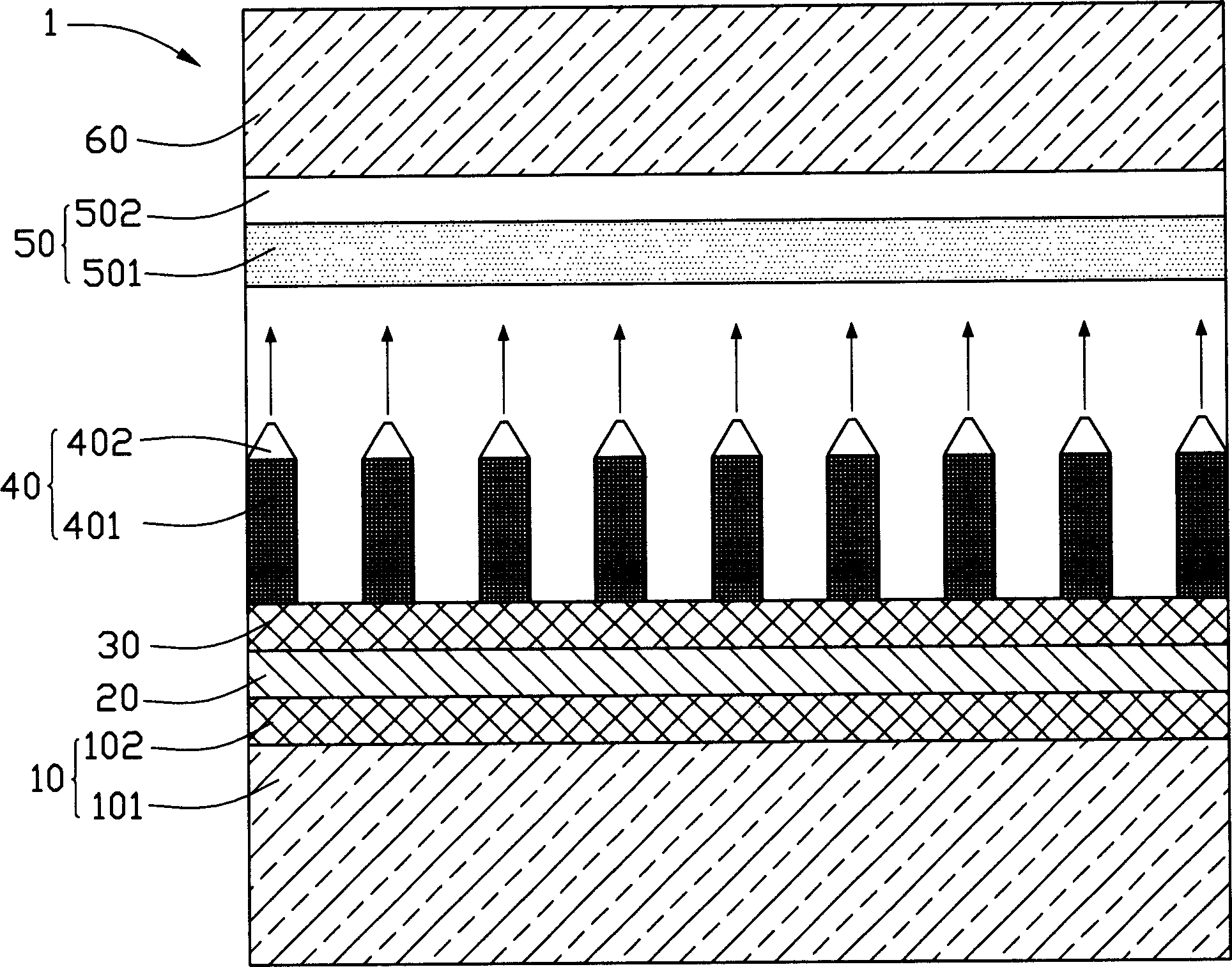
[0015] see figure 1 The field emission display element 1 of the present invention comprises a first substrate 10, a cathode plate 20 made of conductive material and formed on the first substrate 10, a resistor buffer layer 30 connected to the cathode plate 20, formed on the resistor A plurality of electron emission units 40 on the buffer layer 30 , an anode plate 50 spaced apart from the plurality of electron emission units 40 , and a second substrate 60 .

[0016] The first substrate 10 includes a glass substrate 101 and a silicon thin film layer 102, the silicon thin film layer 102 is formed on the glass substrate 101, the silicon thin film layer 102 has bonding properties, which can provide effective bonding between the cathode plate 20 and the glass substrate 101. connect.

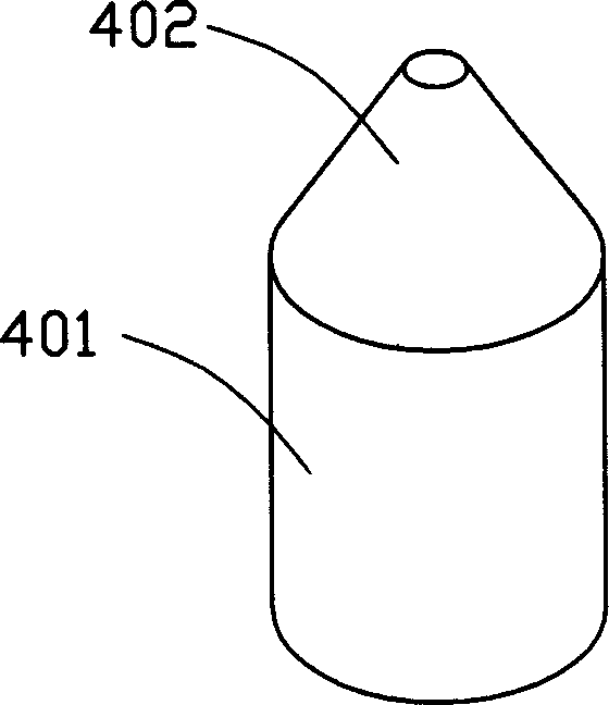
[0017] Please refer to figure 2 , each electron emission unit 40 is composed of a columnar first part 401 in contact with the resistance buffer layer 30 and a conical second part 402 away from the ...


PUM


Abstract

A field emission display device (1) includes a cathode plate (20), a resistive buffer (30) in contact with the cathode plate, a plurality of electron emitters (40) formed on the buffer, and an anode plate (50) spaced from the electron emitters. Each electron emitter includes a rod-shaped first part (401) and a conical second part (402). The buffer and first parts are made from silicon oxide. The combined buffer and first parts has a gradient distribution of electrical resistivity such that highest electrical resistivity is nearest the cathode plate and lowest electrical resistivity is nearest the anode plate. The second parts are made from niobium. When emitting voltage is applied between the cathode and anode plates, electrons emitted from the electron emitters traverse an interspace region and are received by the anode plate. Because of the gradient distribution of electrical resistivity, only a very low emitting voltage is needed.

Description

【Technical field】 [0001] The invention relates to a field emission display element, in particular to a field emission display element which realizes low energy consumption by means of nanoscale electron emission units. 【Background technique】 [0002] In recent years, flat panel displays have developed rapidly and have been widely used in fields such as personal computers and consumer electronics products. At present, the most widely used flat-panel display is an active matrix liquid crystal display with high resolution, hereinafter referred to as liquid crystal display, which can provide high resolution, so it is widely used. However, the inherent limitations of liquid crystal display itself make it unsuitable in some applications. Liquid crystal displays, for example, suffer from a number of manufacturing drawbacks, including slow deposition of amorphous silicon on glass panels and low yields. Moreover, the liquid crystal display requires a high-energy backlight source, b...

Claims


Application Information

Patent Timeline
Patent Type & Authority Applications(China)
IPC IPC(8): H01J1/30H01J1/304H01J29/04H01J31/12H01L29/06H01L31/20
CPCH01J31/127H01J2201/30446Y10S977/952H01J1/3044
Inventor 陈杰良
Owner HONG FU JIN PRECISION IND (SHENZHEN) CO LTD
Why Eureka
Try Eureka