Solid electronic image inductor and control method thereof

A technology of electronic image and sensing device, which is applied in the field of solid electronic image sensing device and its control, can solve the problems of scene limitation of flash photography and achieve the effect of shortening the frame lag

Inactive Publication Date: 2003-07-09
FUJIFILM CORP
View PDF0 Cites 8 Cited by
  • Summary
  • Abstract
  • Description
  • Claims
  • Application Information

AI Technical Summary

Problems solved by technology

Therefore, flash photography scenes are sometimes limited when the frame lag is long

Method used


Image

  • Solid electronic image inductor and control method thereof
  • Solid electronic image inductor and control method thereof
  • Solid electronic image inductor and control method thereof

Examples


Embodiment Construction

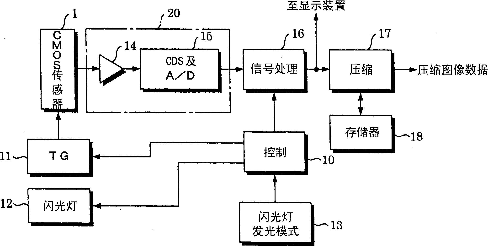
[0029] figure 1 It is a block diagram showing the electrical configuration of a digital camera with a CMOS image sensor.

[0030] The digital camera uses the control circuit 10 to uniformly control the actions of the whole machine.

[0031] The digital camera 1 is provided with a flash light emitting device 12 so that flash photography can be performed. The flash light emitting mode can be set by the flash light emitting mode switch 13. When the signal indicating the flash light emitting mode signal is input to the control circuit 13, the flash light emitting mode is entered, and the flash light emitting device 12 emits light according to the shooting time (details of the flash light emitting time will be described later).

[0032] Various clock pulses and the like are output from the timing generator 11 and supplied to the CMOS image sensor 1. The driving of the CMOS image sensor 1 is controlled by various clock pulses provided by the timing generator 11.

[0033] When the shoo...


PUM


Abstract

In order to reduce the frame rate, when all photodiodes contributing to output of a video signal in a CMOS image sensor must be simultaneously exposed (at the timing of strobe flashing Deltats), as in a case where strobe is flashed, readout pixels composing the CMOS type image sensor are thinned such that the number of photodiodes contributing to the video signal outputted from the CMOS type image sensor is reduced. A time period Deltatp2 required for processing (of the video signal caused by a row of photodiodes) in an analog processing circuit connected to the succeeding stage of the CMOS type image sensor is shortened, thereby reducing the frame rate.

Description

Technical field [0001] The invention relates to a solid electronic image sensing device and a control method thereof, and an electronic camera using the solid electronic image sensing device. Background technique [0002] Image sensors such as CMOS (Complementary Metal-Oxide Semiconductor) type and CCD (Charge Coupled Device) type output the signal charges stored in the photoelectric conversion element sequentially as image signals of one frame in line units. The image signal output by the image sensor is input to analog processing circuits such as an amplifier circuit, a correlation sub-sampling circuit, and an analog / digital conversion circuit. Before the analog processing in the analog processing circuit ends, the image signal of the next frame cannot be input to the analog processing circuit. The analog processing circuit has a relatively slow processing speed, so the time (frame lag) until the next frame of image signal can be output is longer. [0003] In particular, when t...

Claims


Application Information

Patent Timeline
Patent Type & Authority Applications(China)
IPC IPC(8): H04N5/235H04N5/341H04N5/345H04N5/353H04N5/369H04N5/3745H04N9/04
CPCH04N5/2354H04N5/3456H04N5/3454H04N9/045H04N5/3532H04N5/3745H04N23/63H04N23/74H04N25/445H04N25/443H04N25/531H04N25/70H04N25/77H04N25/134
Inventor 西纳直行内山浩行小谷高秋木村壮一郎
Owner FUJIFILM CORP
Why Eureka
Try Eureka