
Conductive element and liquid crystal display with said conductive element

A liquid crystal display and conductive element technology, applied in the field of liquid crystal displays, can solve the problems of increased number of parts, increased assembly steps of assembled parts, space difficulties, etc.

Inactive Publication Date: 2003-06-11
SAMSUNG DISPLAY CO LTD
View PDF0 Cites 5 Cited by
  • Summary
  • Abstract
  • Description
  • Claims
  • Application Information

AI Technical Summary

Problems solved by technology

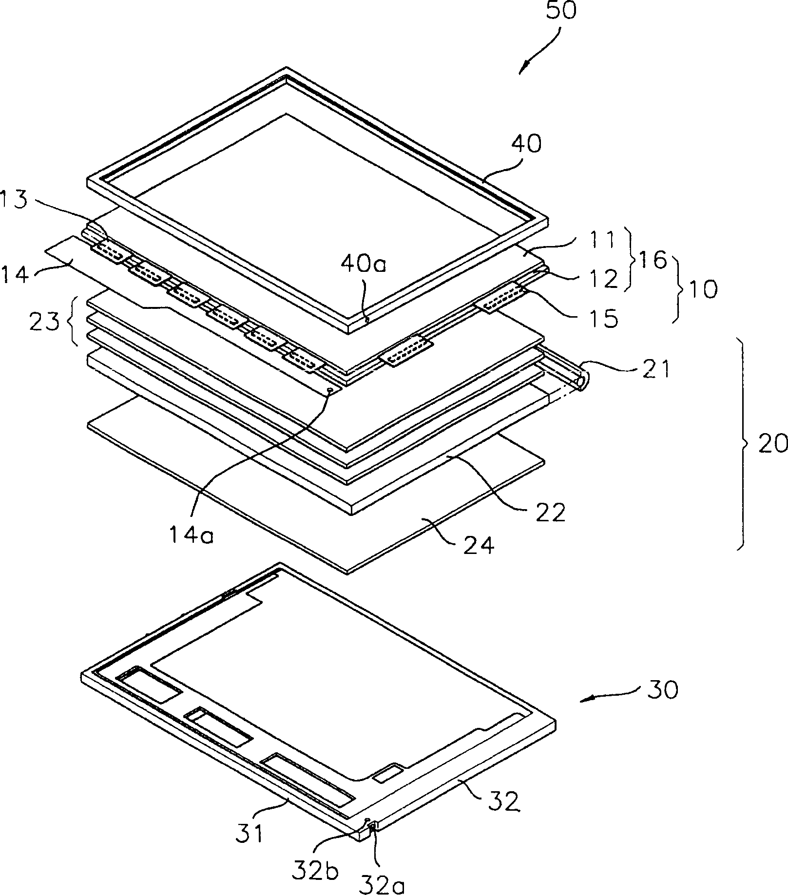
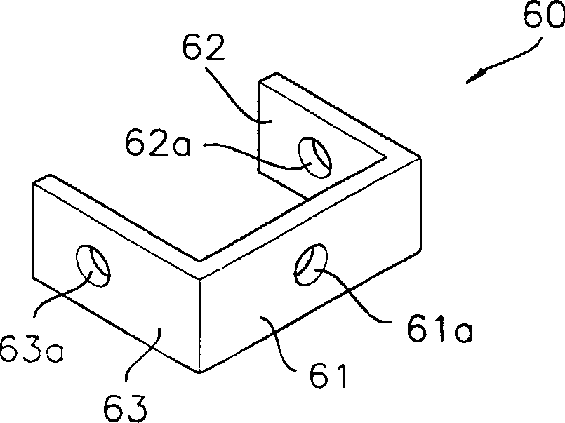
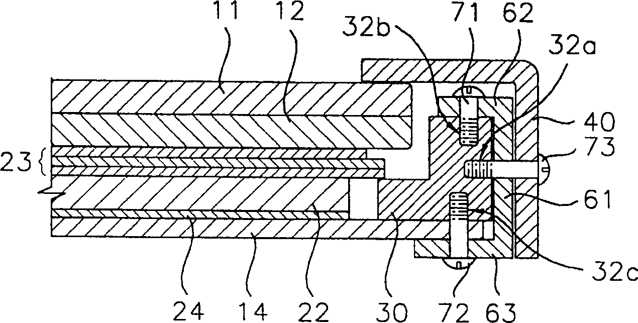
[0019] However, if screws are used to maintain a firm fit and a conductive state of the ground clip 60, because the number of screws increases, the number of parts of the LCD increases, and the number of assembly steps to assemble the parts also increases.
[0020] In addition, in order to make the LCD 50 thinner recently, the thickness of the side wall of the frame 30 has become thinner and thinner, so the mutual coverage area between the ground clip 60 and the side wall of the frame 30 is reduced, which makes it possible to ensure fastening first, Space for the second and third screws 71, 72 and 73 becomes difficult

Method used


Image

  • Conductive element and liquid crystal display with said conductive element
  • Conductive element and liquid crystal display with said conductive element
  • Conductive element and liquid crystal display with said conductive element

Examples


Embodiment Construction

[0039] Exemplary embodiments of the present invention will be described in detail below with reference to the accompanying drawings.

[0040] Figure 4 is an exploded perspective view of an LCD according to an embodiment of the present invention;

[0041] refer to Figure 4 , LCD500 comprises: the display unit 100 of displaying image, the backlight assembly 200 that provides light to display unit 100, the frame 300 that installs display unit 100 and backlight assembly 200, the base plate 400 that display unit 100 is fixed on the frame 300. Although not shown in the drawings, the LCD 500 is installed in front and rear cases (not shown).

[0042] The display unit 100 includes an LCD panel 160 and an integrated PCB 140 that controls the operation of the LCD panel 160 .

[0043] The LCD panel 160 has a thin film type semiconductor substrate 120, a color filter substrate 110 disposed facing the thin film type semiconductor substrate 120, and a liquid crystal layer (not shown) fo...


PUM


Abstract

Disclosed are a conductive member and an LCD having the same. The conductive member functions to fix an integrated PCB, which has a circuit part for controlling an operation of an LCD panel, to a rear surface of a mold frame, and to electrically connect the PCB to a top chassis. The conductive member includes a body portion to contact a sidewall of the mold frame, a first wing portion extended from a first end of the body portion to be coupled with an upper surface of the sidewall of the mold frame, and a second wing portion extended from a second end of the body portion to be coupled with a rear surface of the integrated PCB. Where the conductive member is at a free-existing state, a distance between free ends of the first and second wing portions is less than a distance between the first and second ends of the body portion. Therefore, where the conductive member is coupled with the mold frame and the PCB, a tension generated by a restoring force of the first and second wing portions is exerted on the mold frame and the integrated PCB. Therefore, the conductive member stably fixes the integrated PCB to the rear surface of the mold frame without using a separate fixing member.

Description

technical field [0001] The present invention relates to a conductive element and a liquid crystal display having the conductive element, in particular to such a conductive element and a liquid crystal display in which the number of parts and assembly steps are reduced and the liquid crystal display is lighter and thinner. Background technique [0002] In today's information-oriented society, electronic displays play an increasingly important role, and various electronic display devices are widely used in different industrial fields. Due to the rapid development of semiconductor technology, various information processing devices have become smaller in size and lighter in weight, so the present invention provides a display device with smaller and lighter attributes and low power consumption. [0003] A liquid crystal display includes two substrates in which electrodes are formed and liquid crystal interposed therebetween. A liquid crystal display is a ...

Claims


Application Information

Patent Timeline
Patent Type & Authority Applications(China)
IPC IPC(8): G02F1/1333G02F1/13G02F1/133G02F1/1343G02F1/1345H01L21/60
CPCG02F1/13452G02F1/133
Inventor 李相德
Owner SAMSUNG DISPLAY CO LTD
Learn More