
Hierarchical built-in self-test for system-on-chip design

A technology with built-in self-test and chip, applied in electronic circuit testing, detecting faulty computer hardware, measuring electricity, etc., can solve problems such as no BIST design

Inactive Publication Date: 2007-02-28
GLOBALFOUNDRIES INC
View PDF1 Cites 0 Cited by
  • Summary
  • Abstract
  • Description
  • Claims
  • Application Information

AI Technical Summary

Problems solved by technology

Additionally, there are no known BIST designs for analog, radio frequency (RF), and mixed-signal macros

Method used


Image

  • Hierarchical built-in self-test for system-on-chip design
  • Hierarchical built-in self-test for system-on-chip design
  • Hierarchical built-in self-test for system-on-chip design

Examples


Embodiment Construction

[0064] best practice

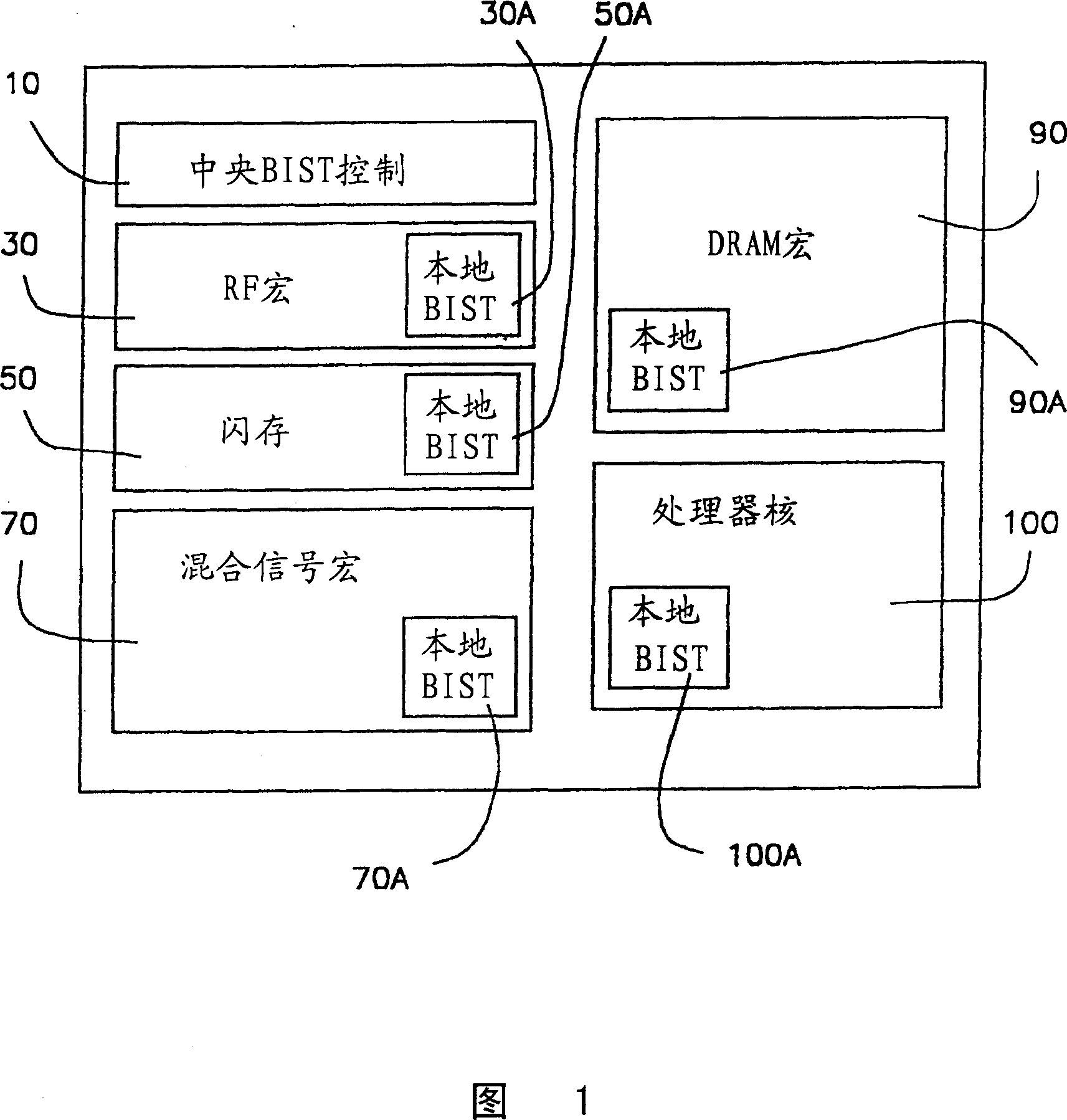
[0065] Figure 1 shows a system-on-chip (SOC) design with specific built-in self-test (BIST) cells. Specifically, the central BIST control unit 10 sends information including address bits and command bits to the local BIST units 30a, 50a, 70a, 90a, 100a of the respective macros 30, 50, 70, 90, 100, respectively, preferably with The following tests are conducted in a graded manner:

[0066] - unit testing of radio frequency (RF) macro 30, flash memory macro 50, mixed signal macro 70, dynamic random access memory macro 90, and processor macro 100;

[0067] - interface testing between the processor macro 100 and the DRAM macro 90, such as reading data from the DRAM to the processor, writing data from the processor to the DRAM, and executing processor test programs from the DRAM macro;

[0068] - Interface test between RF macro 30 and external antenna;

[0069] - Interface testing between the RF macro 30 and the base-band part of the mixed-signal macro 70;...


PUM


Abstract

Hierarchical built-in self-test methods and arrangement for verifying system functionality. As a result, an effective built-in self-test methodology is provided for conducting complete system-on-chip testing, to ensure both the circuit reliability and performance of system-on-chip design. As an added advantage, development costs are reduced for system-on-chip applications.

Description

field of invention [0001] The present invention generally relates to built-in-self-test in and for computer chips. technical background [0002] Built-in self-test (BIST) designs are already common practice in new chips for memory and microprocessors. Some BIST designs are used only once during wafer-level or module-level testing to screen out bad chips. Other BIST designs are used throughout the lifetime of the chip to self-test and repair after each power-on. In today's high-density, high-performance chip design, BIST has become a key circuit component that determines product development costs and time-to-market. [0003] A typical BIST circuit in a high density dynamic random access memory (DRAM) includes a controller, cache memory, pattern generator and data comparator. (For example, see "Processor-based built-in Self-test for Embedded DRAM" by Jeffery Dreibeibis et al., IEEE Journal of Solid State Circuits, Vol. 33, No. 11, 1988, pp. 1731-1739.) Signals for the contr...

Claims


Application Information

Patent Timeline
Patent Type & Authority Patents(China)
IPC IPC(8): G06F11/27G01R31/3187G01R31/28G06F11/22H01L21/822H01L27/04
CPCG06F11/27
Inventor H·H·陈L·L·-C·许L·-K·王
Owner GLOBALFOUNDRIES INC
Learn More