
Photosensitive element substrate

A technology for photosensitive elements and substrates, which can be used in electrical components, semiconductor devices, radiation control devices, etc., and can solve problems such as poor electrical properties of transistors

Pending Publication Date: 2022-07-05
AU OPTRONICS CORP
View PDF0 Cites 0 Cited by
  • Summary
  • Abstract
  • Description
  • Claims
  • Application Information

AI Technical Summary

Problems solved by technology

However, during the manufacturing process, the operational electrical properties of the metal oxide semiconductor layer, such as the current-voltage curve (I-V curve), are easily affected by the reaction gas of the subsequent manufacturing process and change, resulting in poor electrical properties of the subsequently formed transistors.

Method used


Image

  • Photosensitive element substrate
  • Photosensitive element substrate
  • Photosensitive element substrate

Examples


Embodiment Construction

[0037] As used herein, "about", "approximately", "substantially", or "substantially" includes the stated value and the average value within an acceptable deviation of the particular value as determined by one of ordinary skill in the art, taking into account all The measurement in question and the specific amount of error associated with the measurement (ie, the limitations of the measurement system). For example, "about" can mean within one or more standard deviations of the stated value, or within ±30%, ±20%, ±15%, ±10%, ±5%, for example. Furthermore, "about", "approximately", "substantially", or "substantially" as used herein may be used to select a more acceptable range of deviation or standard deviation depending on the nature of measurement, cutting nature or other properties, rather than One standard deviation applies to all properties.

[0038] In the drawings, the thickness of layers, films, panels, regions, etc., are exaggerated for clarity. It will be understood t...


PUM


Abstract

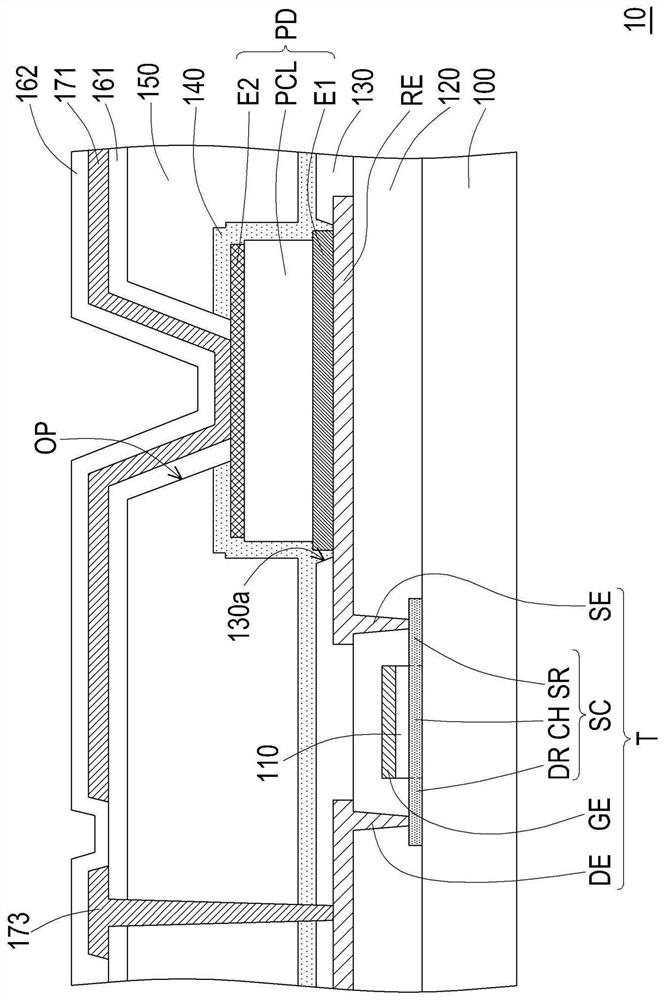
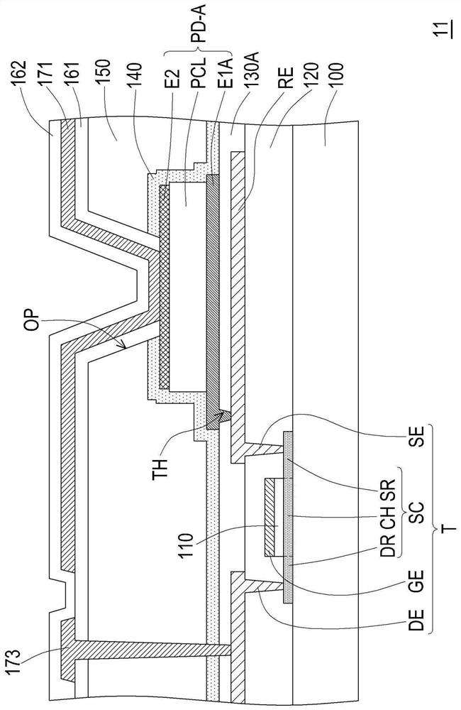
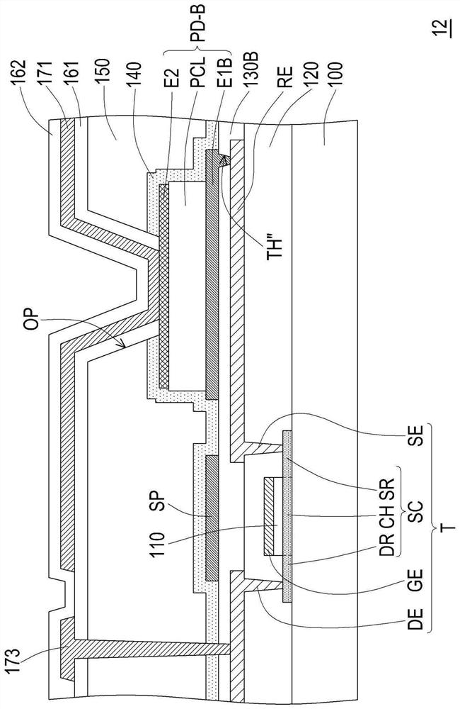
The invention discloses a photosensitive element substrate. The photosensitive element substrate comprises a substrate, an active element and a photosensitive element, the active element and the photosensitive element are arranged on the substrate. The active element has a semiconductor pattern and a gate. The semiconductor pattern is disposed between the substrate and the gate. The photosensitive element is electrically connected with the active element. The photosensitive element has a photoelectric conversion layer, and a first electrode and a second electrode disposed on opposite sides of the photoelectric conversion layer. The first electrode is located between the photoelectric conversion layer and the semiconductor pattern, and the material of the first electrode includes a metal oxide.

Description

technical field [0001] The present invention relates to a sensing substrate, and in particular, to a photosensitive element substrate. Background technique [0002] The applications of light sensors are very extensive. Commonly used image sensors for digital cameras or video cameras, such as complementary metal-oxide-semiconductor (Complementary Metal-Oxide-Semiconductor, CMOS) image sensors or charge-coupled device (Charge-coupled Device, CCD) image sensors. In addition, non-visible light (such as X-ray) sensors for security inspection, industrial inspection or medical diagnosis have become the key development projects of relevant manufacturers due to their high added value. [0003] Generally speaking, X-ray sensors used for medical testing or surgery must have a high sensing frequency so that medical personnel can obtain the real-time state of the patient's body from it, so as to increase the accuracy of detection and the success rate of surgery. Therefore, most of thes...

Claims


Application Information

Patent Timeline
Patent Type & Authority Applications(China)
IPC IPC(8): H01L27/146H01L31/0224H01L31/102
CPCH01L27/14643H01L27/14612H01L31/022408H01L31/102H01L31/1055H01L31/056H01L27/14658H01L31/0328H01L31/109
Inventor 蔡佳修张家铭陈瑞沛
Owner AU OPTRONICS CORP
Learn More