Defect detection method, device and equipment and computer readable storage medium

A defect detection and defect technology, applied in the field of detection, can solve problems affecting the use function of functional areas, pits or protrusions in functional areas, etc., to improve detection accuracy, avoid re-inspection, and improve detection efficiency.

Pending Publication Date: 2022-04-12
SKYVERSE TECH CO LTD
View PDF0 Cites 0 Cited by
  • Summary
  • Abstract
  • Description
  • Claims
  • Application Information

AI Technical Summary

Problems solved by technology

[0002] In the wafer manufacturing process, different types of defects often appear in different functional areas of the wafer, especially for wafers with patterns. Due to the influence of manufacturing process or other factors, the functional areas on the patterned wafer often have defects such as pits or bumps, which affect the use of functional areas

Method used


Image

  • Defect detection method, device and equipment and computer readable storage medium
  • Defect detection method, device and equipment and computer readable storage medium
  • Defect detection method, device and equipment and computer readable storage medium

Examples


Embodiment Construction

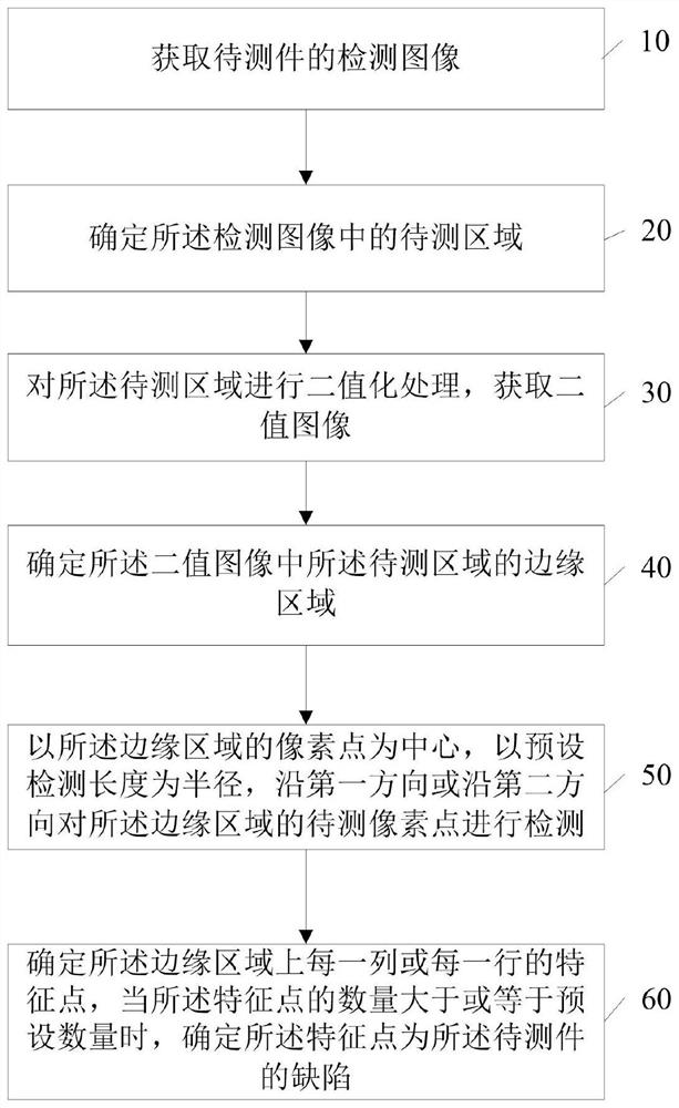
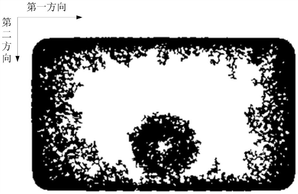
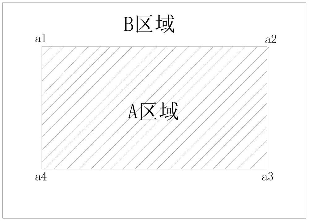
[0048] In order to enable those skilled in the art to better understand the solution of the present application, the technical solution in the embodiment of the application will be clearly and completely described below in conjunction with the accompanying drawings in the embodiment of the application. Obviously, the described embodiment is only It is an embodiment of a part of the application, but not all of the embodiments. Based on the embodiments in this application, all other embodiments obtained by persons of ordinary skill in the art without creative efforts shall fall within the scope of protection of this application.

[0049] Each will be described in detail below.

[0050] The terms "first", "second", "third" and "fourth" in the specification and claims of this application and the drawings are used to distinguish different objects, rather than to describe a specific order . Furthermore, the terms "include" and "have", as well as any variations thereof, are intende...


PUM


Abstract

The invention discloses a defect detection method, device and equipment and a computer readable storage medium. The defect detection equipment obtains a detection image of a to-be-detected piece; determining a to-be-detected area of the detection image; performing binarization processing on the to-be-detected area to obtain a binary image; determining an edge region in the binary image, wherein the edge region comprises white pixel points of a plurality of regions to be detected; detecting the pixel points to be detected in the edge area along the first direction or the second direction; and determining feature points of each column or each row on the edge area, and when the number of the feature points is greater than or equal to a preset number, determining that the feature points are defects of the to-be-detected piece. By determining the edge area of the to-be-detected area on the wafer, determining the feature points on the edge area and then determining the defect of the to-be-detected piece according to the feature points, the defect type on the to-be-detected piece can be accurately determined through the positions of the feature points, the detection accuracy of the to-be-detected piece is improved, reinspection caused by low detection accuracy is avoided, and the detection accuracy of the to-be-detected piece is improved. And the detection efficiency of the to-be-detected piece is improved.

Description

technical field [0001] The present application relates to the technical field of detection, and in particular to a defect detection method, device, equipment and computer-readable storage medium. Background technique [0002] In the wafer manufacturing process, different types of defects often appear in different functional areas of the wafer, especially for wafers with patterns. Due to the influence of the manufacturing process or other factors, the functional areas on the patterned wafer often have defects such as pits or protrusions, which affect the use of the functional areas. [0003] In the prior art, when performing defect detection on a wafer, it is usually necessary to use a template image to compare the detection image of the wafer with the template image. When the detection image matches the template image to a high degree, it is determined that the wafer meets the requirements for use. It is required that when the matching degree between the detection image and...

Claims


Application Information

Patent Timeline
Patent Type & Authority Applications(China)
IPC IPC(8): G06T7/00G06T7/62G06T7/66
Inventor 陈鲁肖遥佟异张嵩
Owner SKYVERSE TECH CO LTD
Why Eureka
Try Eureka