Fixture and method for detecting full-size position of whole substrate product
A technology for detecting fixtures and substrates, applied in the field of solder printing, can solve the problems of unguaranteed accuracy and damage to the entire substrate product, and achieve the effect of convenient material retrieval.
- Summary
- Abstract
- Description
- Claims
- Application Information
AI Technical Summary
Problems solved by technology
Method used
Image
Examples
Embodiment 1
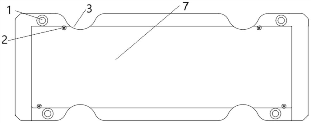
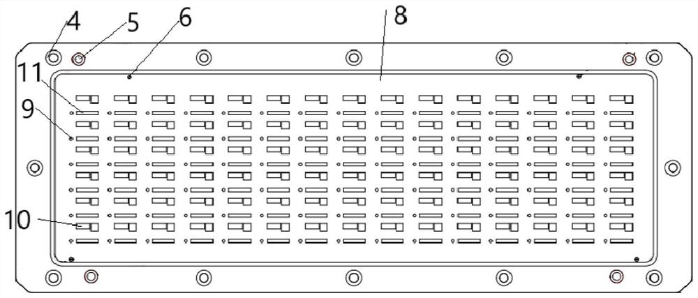
[0032] A fixture for detecting the size and position of a whole substrate product, comprising a detection base 7 and a detection cover 8, the detection cover 8 is arranged above the detection base 7, and the detection cover 8 is provided with a plurality of foot points 9, characters 11 and several detection holes 10, the characters 11 and the first foot point 9 have the same number, each character 11 and a first foot point 9 correspond to a group, and each group of characters 11 and the first foot point 9 corresponds to a detection hole 10 .
[0033] The detection base 7 is rectangular, and the detection base 7 is provided with four grooves 3, and each long side of the detection base 7 is provided with 2 grooves 3, and the grooves 3 on the two long sides are mutually symmetrical, and the grooves 3 is used to take away the entire substrate product from the groove 3 after the inspection is completed.
[0034] Four screws 1 are uniformly arranged around the detection base 7 to f...
Embodiment 2
[0044] A method for detecting the size and position of a whole substrate product, based on a jig for detecting the size and position of a whole substrate product in Embodiment 1, comprising the following steps:
[0045] Firstly, put the entire substrate product on the detection base 7, and cover the detection cover plate 8; make the concave first positioning pin 2 and the convex second positioning pin 5 cooperate;
[0046] Secondly, stick the positioning pin 6 on the positioning hole of the entire substrate product for positioning adjustment until the first foot point 9 is aligned with the reference first foot point on the entire substrate product;
[0047] Then, observe from the detection hole 10 whether the printing area on the entire substrate product is offset;
[0048] Finally, when the detection is completed, the detection cover 8 is removed, and the entire printed substrate product is removed from the groove 3 .
PUM
 Abstract
Description
Claims
Application Information
 - R&D Engineer
- R&D Manager
- IP Professional
- Industry Leading Data Capabilities
- Powerful AI technology
- Patent DNA Extraction
Browse by: Latest US Patents, China's latest patents, Technical Efficacy Thesaurus, Application Domain, Technology Topic, Popular Technical Reports.
© 2024 PatSnap. All rights reserved.Legal|Privacy policy|Modern Slavery Act Transparency Statement|Sitemap|About US| Contact US: help@patsnap.com


