Appearance defect detection equipment and detection method thereof

A technology for appearance defects and detection equipment, which is applied in optical testing flaws/defects, measuring devices, material analysis by optical means, etc. High requirements, to achieve the effect of being conducive to large-scale testing, high work efficiency, and improving the degree of automation

Pending Publication Date: 2022-03-01
皓星智能装备(东莞)有限公司
View PDF0 Cites 0 Cited by
  • Summary
  • Abstract
  • Description
  • Claims
  • Application Information

AI Technical Summary

Problems solved by technology

[0003] In the traditional technology, the detection of wafer appearance defects is usually carried out by manual inspection of the wafer with the naked eye. This detection method is inefficient, labor-intensive, and prone to false detection or missed detection. The quality of wafer products; later, testing equipment for automatic detection of wafers appeared, which can improve the detection efficiency and quality of detection, but for the high demand for neat arrangement and extremely low false detection rate (almost zero false detection and missed detection rate). still unsatisfactory

Method used


Image

  • Appearance defect detection equipment and detection method thereof
  • Appearance defect detection equipment and detection method thereof
  • Appearance defect detection equipment and detection method thereof

Examples


Embodiment Construction

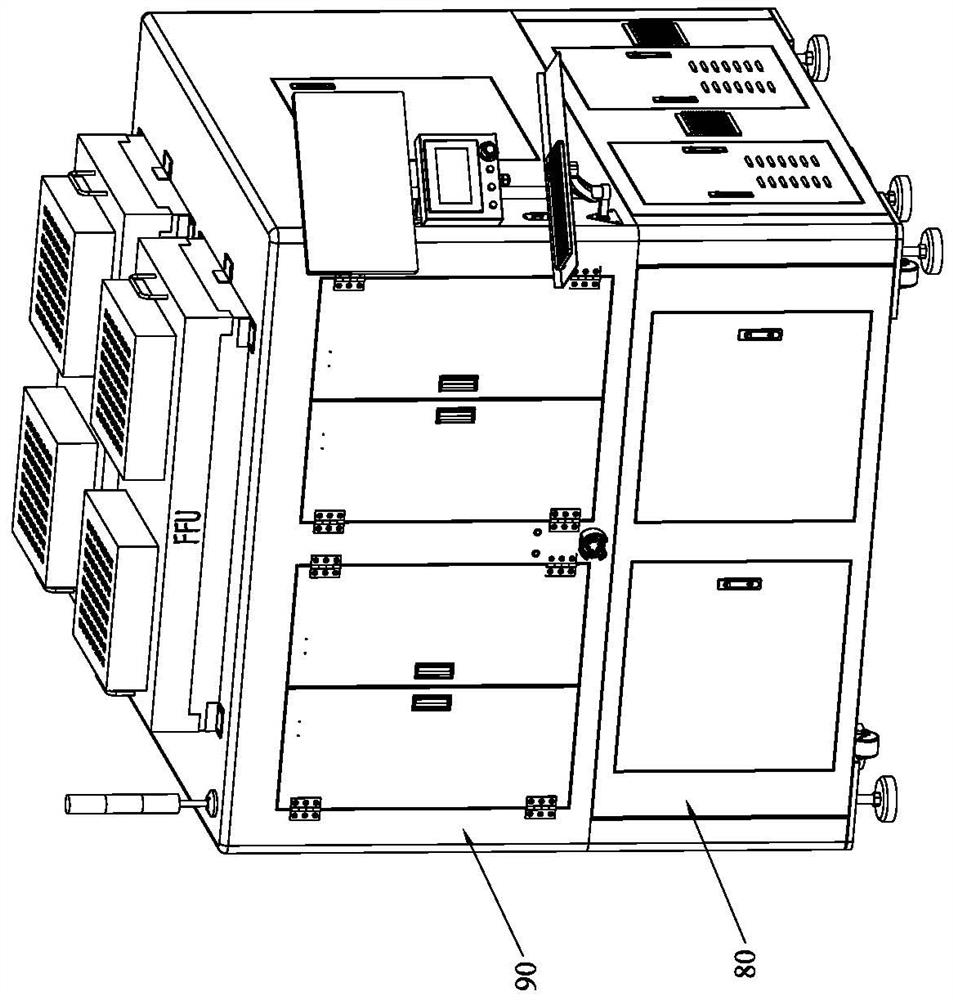
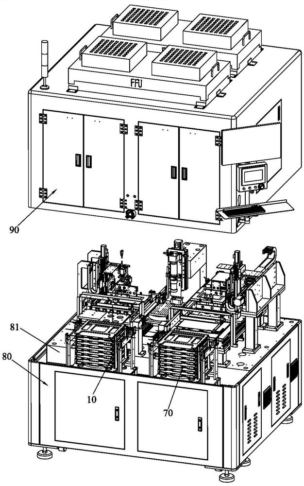
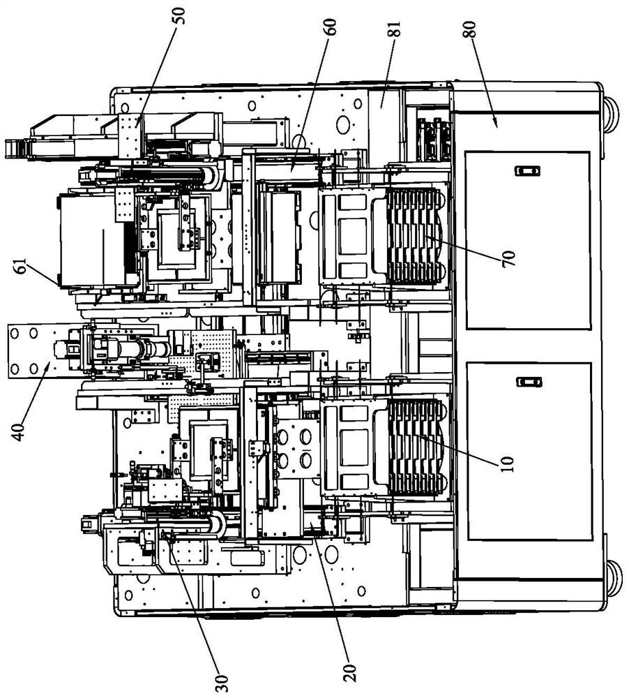
[0061] Please refer to Figure 1 to Figure 11As shown, it has shown the specific structure of a preferred embodiment of the present invention, including a feeding tray warehouse 10, a feeding and transplanting device 20, a feeding conversion mechanism 30, a CCD detection mechanism 40, and a feeding conversion mechanism arranged in sequence. Mechanism 50, blanking and transplanting device 60 and blanking tray warehouse 70;

[0062] Both the loading and transplanting device 20 and the blanking and transplanting device 60 are arranged along the X axis, and the loading and transferring mechanism 30 and the unloading and converting mechanism 50 are arranged on the loading and transplanting device 20 and the blanking and transplanting device respectively. On the outside of the device 60 , the CCD detection mechanism 40 is arranged between the inside of the loading and transplanting device 20 and the inside of the unloading and transplanting device 60 .

[0063] The loading and tran...


PUM


Abstract

The invention discloses appearance defect detection equipment and a detection method thereof. The appearance defect detection equipment comprises a feeding disc bin, a feeding transplanting device, a feeding conversion mechanism, a CCD detection mechanism, a discharging conversion mechanism, a discharging transplanting device and a discharging disc bin which are sequentially arranged. Each of the feeding conversion mechanism and the discharging conversion mechanism comprises a taking and placing device and a first Z-axis driving device for driving the taking and placing device to do lifting motion; the CCD detection mechanism comprises a detection station and a CCD detection Z-axis module, the CCD detection Z-axis module comprises a second Z-axis driving device and a CCD detection device arranged on the second Z-axis driving device, and the CCD detection Z-axis module is arranged corresponding to the detection station. The detection station is connected between the feeding switching mechanism and the discharging switching mechanism through an XY theta axial driving mechanism. The automatic detection of the product is realized, the working efficiency is high, the detection quality is high, the labor cost is saved, and the large-batch detection of the product is facilitated.

Description

technical field [0001] The invention relates to the technology in the field of detection equipment, in particular to an appearance defect detection equipment and a detection method thereof, which are mainly used for wafer appearance detection. Background technique [0002] The wafer manufacturing process is also constantly improving. In order to effectively ensure the yield rate of wafer products, it is often necessary to inspect the appearance of the wafer for defects after the wafer is manufactured and formed. [0003] In traditional technology, the detection of wafer appearance defects is usually done manually with the naked eye. This detection method is inefficient, labor-intensive, and prone to false detection or missed detection. The quality of wafer products; later, testing equipment for automatic detection of wafers appeared, which can improve the detection efficiency and quality of detection, but for the high demand for neat arrangement and extremely low false detec...

Claims


Application Information

Patent Timeline
Patent Type & Authority Applications(China)
IPC IPC(8): G01N21/89
CPCG01N21/8914
Inventor 陈祖华袁璐奇
Owner 皓星智能装备(东莞)有限公司
Why Eureka
Try Eureka