
Feeding and discharging device of semiconductor packaging material box

A packaging material and semiconductor technology, used in semiconductor/solid-state device manufacturing, transportation and packaging, lighting and heating equipment, etc., can solve problems such as complex structure, substrate scratches, pressure injuries, etc., to achieve simple and reliable mechanism and reduce production. Cost, loss reduction effect

Pending Publication Date: 2022-01-04
深圳市矽谷半导体设备有限公司
View PDF0 Cites 0 Cited by
  • Summary
  • Abstract
  • Description
  • Claims
  • Application Information

AI Technical Summary

Problems solved by technology

At present, the existing wafer loading and unloading settings mainly use the way of stacking materials for loading and receiving. Such a feeding method is prone to scratches or crushing of the substrate. Of course, a small number of them use the lifting mechanism to directly drive the material box up and down. It realizes feeding and receiving, but its structure is complicated, it is inconvenient to load and receive materials, and it cannot be adapted to different sizes of material boxes, so it is necessary to improve

Method used


Image

  • Feeding and discharging device of semiconductor packaging material box
  • Feeding and discharging device of semiconductor packaging material box
  • Feeding and discharging device of semiconductor packaging material box

Examples


Embodiment Construction

[0023] The following are only preferred embodiments of the present invention, and therefore do not limit the protection scope of the present invention.

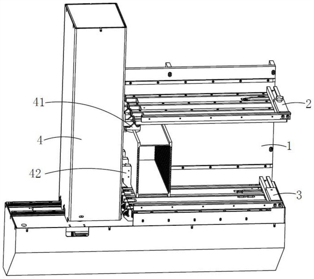
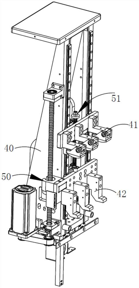
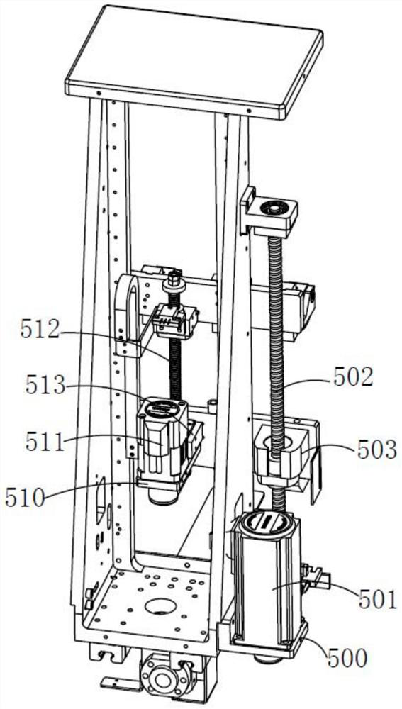
[0024] Such as Figures 1 to 4 As shown, the present invention provides a loading and unloading device for semiconductor packaging magazines, which includes a stand 1, an upper support structure 2 arranged on the top of the stand 1, a lower support structure 3 arranged at the bottom of the stand 1, and a feeding Lifting device 4, feeding lifting device 4 is provided with Z-axis seat 40, lifting drive mechanism, the material box upper clip 41 that is slidably arranged on Z-axis seat 40 tops and the material box lower clip 42 that is slidably arranged on Z-axis seat 40 bottom, material The box upper clamp 41 and the material box lower clamp 42 are arranged up and down to clamp the material box, and the lifting drive mechanism is used to drive the material box upper clamp 41 and the material box lower clamp 42 to lift synchronou...


PUM


Abstract

The invention discloses a feeding and discharging device for a semiconductor packaging material box. The device comprises a vertical seat, an upper-layer supporting structure arranged at the upper part of the vertical seat, a lower-layer supporting structure arranged at the lower part of the vertical seat and a feeding lifting device, the feeding lifting device is provided with a Z-axis base, a lifting driving mechanism, a material box upper clamp arranged on the upper portion of the Z-axis base in a sliding mode and a material box lower clamp arranged on the lower portion of the Z-axis base in a sliding mode, the material box upper clamp and the material box lower clamp are arranged in an up-and-down oppositely-combined mode to be used for clamping the material box, the lifting driving mechanism is used for driving the material box upper clamp and the material box lower clamp to ascend and descend synchronously, and therefore, the material box is driven to be switched between the upper-layer supporting structure and the lower-layer supporting structure. According to the structural design, a plurality of semiconductor wafers can be borne at a time through the material box, the purpose of rapid feeding is achieved, the situation that material pieces are scratched or crushed is avoided, unnecessary losses are reduced, and in addition, switching and compatibility of the material boxes of different specifications can be easily achieved in the mode that the material boxes are distributed in an upper layer and a lower layer.

Description

technical field [0001] The invention relates to the technical field of semiconductor wafer packaging technology, in particular to a loading and unloading device for a semiconductor packaging material box. Background technique [0002] At present, the domestic semiconductor wafer packaging technology is developing rapidly, and the requirements for the appearance and operation convenience of semiconductor die-bonding equipment are getting higher and higher. At present, the existing wafer loading and unloading settings mainly adopt the method of stacking materials for loading and receiving. Such a feeding method is prone to scratches or crushing of the substrate. Of course, a small number of them use a lifting mechanism to directly drive the material box up and down. It realizes feeding and receiving, but its structure is complicated, it is inconvenient to load and receive materials, and it cannot be adapted to material boxes of different sizes, so it is necessary to improve it...

Claims


Application Information

Patent Timeline
Patent Type & Authority Applications(China)
IPC IPC(8): B65G49/07B65G41/00B65G21/12B65G15/30H01L21/677
CPCB65G49/07B65G41/006B65G21/12B65G15/30H01L21/67703
Inventor 刘维强陈勇伶
Owner 深圳市矽谷半导体设备有限公司
Learn More