
Patsnap Eureka
For R&D, Patsnap Eureka makes reading and utilizing patents & technical documents easy.
Patsnap Eureka AIR
Designed for self-driven R&D workflows. Generate viable solutions, solve complex R&D challenges, empower your innovation with AI.

Patsnap Eureka Materials
Designed for material experts only. Revolutionize your material R&D, from search, analyze, to developing new materials.

TechResearch
Generate reliable direction feasibility study reports for your R&D in just a few steps.

TechSeek
Discover and master advanced knowledge NOW. Basics, ideas, possibilities, all at once.

TechMind
As an expert in R&D Theories, TechMind can generates customized viable solutions instantly.

TechRisk
Analyze your overall solution with one click, know your potential R&D risks in advance.

TechMonitor
Get weekly tech updates, stay abreast of the latest tech innovations and key insights.
Silicon wafer material box device
A silicon wafer and material box technology, which is applied in transportation and packaging, conveyor objects, electrical components, etc., can solve the problems of high defect rate, high silicon wafer fragmentation rate, and many cracks, so as to save cost and reduce loss rate. , the effect of reducing crack loss
- Summary
- Abstract
- Description
- Claims
- Application Information
AI Technical Summary
Problems solved by technology
Method used
Image

Examples
Embodiment Construction
[0025] The technical solutions provided by the present invention will be described in detail below in conjunction with the accompanying drawings.
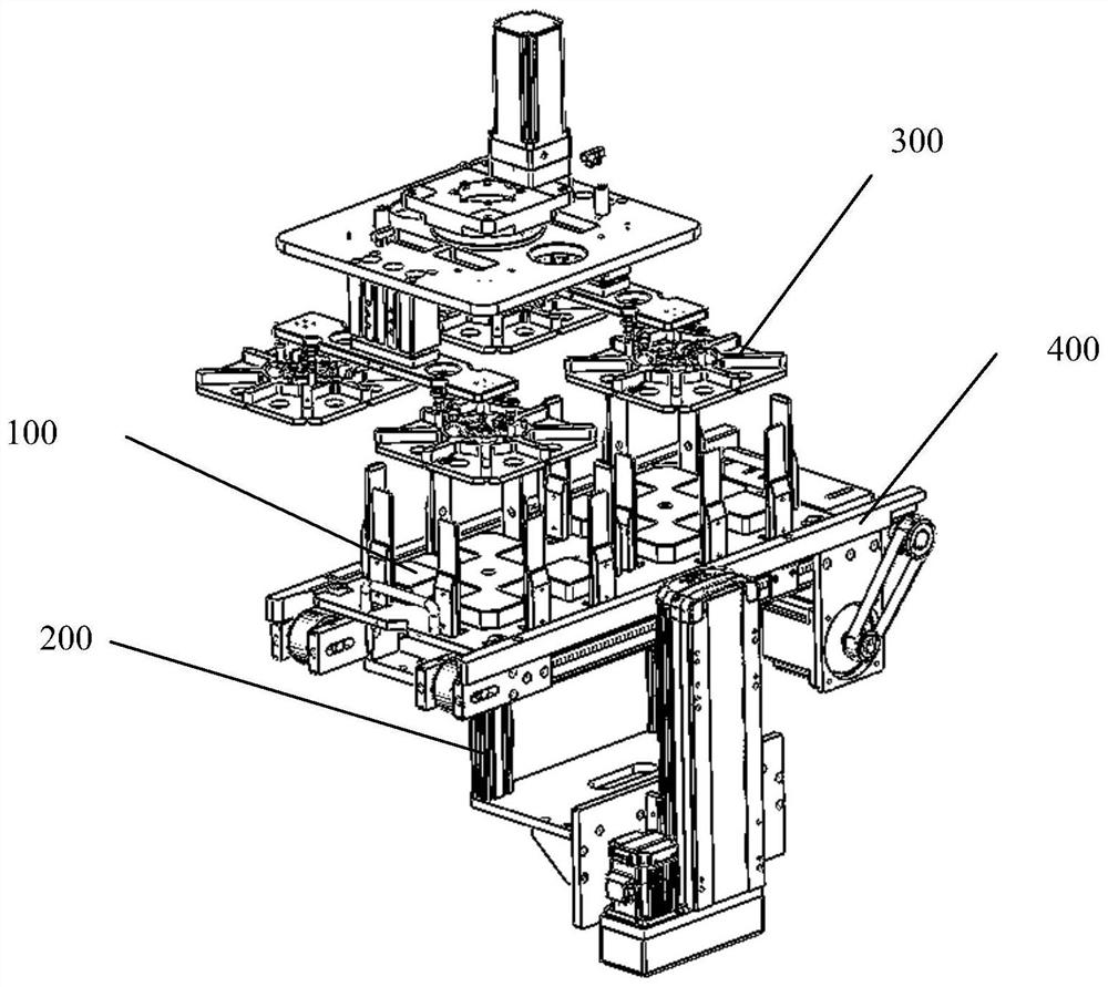
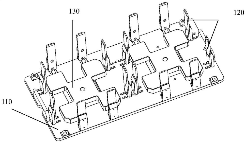
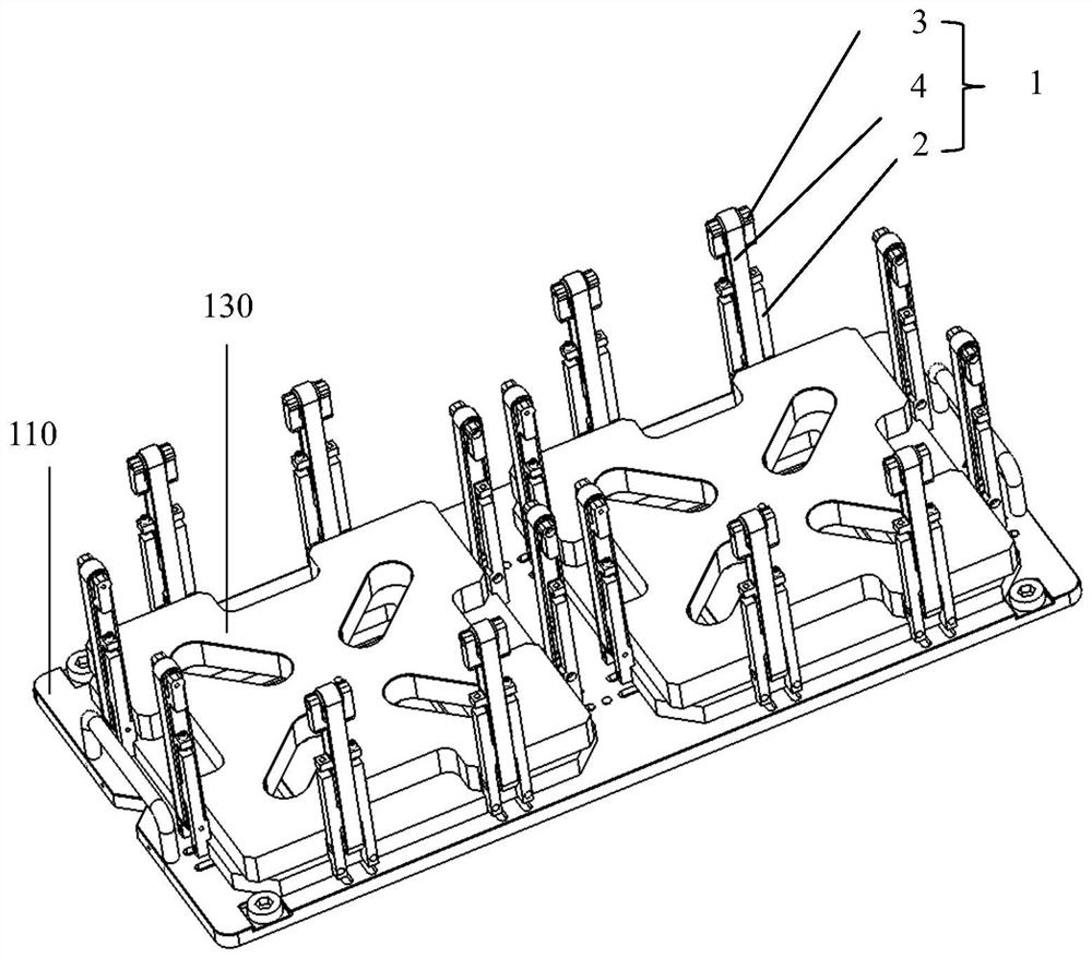
[0026] Such as image 3 As shown, the silicon wafer magazine device includes a bottom plate 110 and a plurality of trays 130 arranged on the bottom plate 110, and also includes a plurality of edge retaining mechanisms 1, and the plurality of edge retaining mechanisms 1 are respectively located around the tray 130. A tray 130 is loaded with silicon wafers. Each edge retaining mechanism 1 comprises a lower guide column 2, an upper guide column 3, a conveyor belt 4, a first pulley 5, and a second pulley 6, wherein the lower guide column 2 is connected with the base plate 110, and the upper guide column 3 is connected with the lower guide post 2 by slipping, the first pulley 5 is set on the lower guide post 2, the second pulley 6 is set on the upper guide post 3, the conveyor belt 4 is connected with the first pulley 5 and the second ...
PUM
 Abstract
Description
Claims
Application Information
 - R&D Engineer
- R&D Manager
- IP Professional
- Industry Leading Data Capabilities
- Powerful AI technology
- Patent DNA Extraction
Browse by: Latest US Patents, China's latest patents, Technical Efficacy Thesaurus, Application Domain, Technology Topic, Popular Technical Reports.
© 2024 PatSnap. All rights reserved.Legal|Privacy policy|Modern Slavery Act Transparency Statement|Sitemap|About US| Contact US: help@patsnap.com