
Display panel and display device

A technology for display panels and display parts, which is applied to identification devices, instruments, etc., can solve problems such as easy falling off of COF, save material costs and labor assembly costs, reduce frame width, and facilitate installation and disassembly.

Active Publication Date: 2021-10-29
HKC CORP LTD
View PDF7 Cites 0 Cited by
  • Summary
  • Abstract
  • Description
  • Claims
  • Application Information

AI Technical Summary

Problems solved by technology

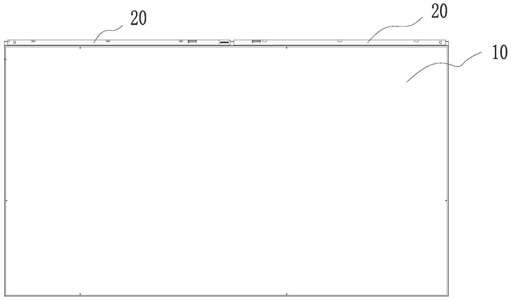
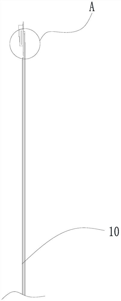
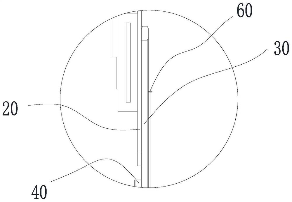
[0004] The purpose of the embodiments of the present application is to provide a display panel and a display device, aiming to solve the problem that the COF is easy to fall off caused by the connection of the display panel to the circuit board through the COF in the prior art

Method used


Image

  • Display panel and display device
  • Display panel and display device
  • Display panel and display device

Examples


Embodiment Construction

[0028] In order to make the technical problems, technical solutions and beneficial effects to be solved by the present application clearer, the present application will be further described in detail below in conjunction with the accompanying drawings and embodiments. It should be understood that the specific embodiments described here are only used to explain the present application, and are not intended to limit the present application.

[0029] It should be noted that when an element is referred to as being “fixed” or “disposed on” another element, it may be directly on the other element or be indirectly on the other element. When an element is referred to as being "connected to" another element, it can be directly connected to the other element or indirectly connected to the other element. In the case of no conflict, the embodiments in the present application and the features in the embodiments can be combined with each other. The present application will be described in ...


PUM


Abstract

The invention is suitable for the technical field of display panels, and provides a display panel and a display device.According to the display panel, a lead connecting structure on an array substrate protrudes out of a color film substrate to form a direct connecting part, and a circuit board and the color film substrate are arranged side by side, so that the circuit board and the array substrate are directly connected to complete electric transmission; therefore, a COF structure is omitted, the frame width of the panel can be greatly reduced, the frame of the display equipment can be made to be narrower than that in the prior art, the omitted COF structure also avoids the problems that the COF is prone to connection failure and falling off. Meanwhile, the material cost and the manual assembly cost of the COF are omitted, and mounting and dismounting are convenient.

Description

technical field [0001] The present application belongs to the technical field of display panels, and more specifically relates to a display panel and a display device. Background technique [0002] Existing display panels usually form a complete whole by thermally bonding CELL (screen module), COF (chip on flex film), and PCBA (Printed Circuit Board Assembly). Structured display panels have significant limitations. [0003] At present, what the wallpaper TV is pursuing is the ultimate thinness. In order to achieve this effect, components such as the motherboard and power board that will affect the thickness of the whole machine are usually placed in the main box outside the backplane. Similarly, the PCBA cannot be installed in the backplane. behind the board, but rests flat on the backplane. Make PCBA and display glass design on the same plane, then the width of PCBA and COF will directly affect the frame width of the whole machine, making the frame width limited. Moreove...

Claims


Application Information

Patent Timeline
Patent Type & Authority Applications(China)
IPC IPC(8): G09F9/30
CPCG09F9/30
Inventor 张双童袁海江
Owner HKC CORP LTD
Learn More