Organomagnesium compounds and electronic devices

A technology of electronic devices and compounds, which is applied in the direction of magnesium organic compounds, electrical components, semiconductor devices, etc., can solve the problems of uneven doping concentration of magnesium on the chip, inability to meet the needs, and only applicable magnesium compounds, etc., to improve the stability of the production process performance, improve the efficiency of gallium production, and the effect of uniform distribution of magnesium components

Active Publication Date: 2021-11-23
JIANGSU NATA OPTO ELECTRONICS MATERIAL
View PDF3 Cites 0 Cited by
  • Summary
  • Abstract
  • Description
  • Claims
  • Application Information

AI Technical Summary

Problems solved by technology

[0004] Magnesium is usually used as a dopant in the epitaxial growth of P-type gallium nitride technology. Magnesium dicene is the most commonly used source of magnesium. Its melting point is greater than 170 ° C. It is a colorless crystal at normal temperature and pressure. As a solid source, magnesium dicene There are many limitations, for example, due to the small surface area of ​​the product particles, and "channeling" is easy to occur in the steel cylinder used, resulting in unstable vapor pressure, uneven doping concentration of magnesium in the prepared chip, and the usage rate of magnesium dicene is lower than 20%
[0005] Solid-state magnesocene can no longer meet the needs of the existing process for large-flow magnesium source steam
In order to solve this problem, the prior art generally optimizes the substituents on the magnesocene ring or the form of the magnesocene. A magnesium compound suitable for atomic layer deposition, the magnesium compound maintains the overall structure of magnesiumocene, and at the same time replaces a hydrogen atom on the magnesiumocene ring with isopropyl, sec-butyl or tert-butyl, but the Magnesium compounds are only suitable for atomic layer deposition
Chinese patent literature (application publication number: CN1399006A, application publication date: February 26, 2003) discloses a method for preparing a solution magnesium source, which disperses magnesium dicene or dimethyl magnesium dicene in a solvent, A high-concentration solution magnesium source is formed to replace the solid-state magnesium dicene, but this method inevitably introduces solvents that interfere with the epitaxy process

Method used


Image

  • Organomagnesium compounds and electronic devices

Examples


preparation example Construction

[0023] The preparation process of the organomagnesium compound shown in structural formula (1) is as follows:

[0024] In an anhydrous and oxygen-free glove box, add 98 g of high-purity magnesium chips into a cylindrical quartz synthesis column with a heating wire, the magnesium chips are held by the baffle in the synthesis column, and the synthesis column is placed vertically; above the synthesis column , connected to a 500 ml constant pressure funnel with a stopcock, 500 ml of methylcyclopentadiene monomer was added to the funnel, and the top of the funnel was connected to an argon cylinder; below the synthesis column, a 2000 ml two-necked flask was connected, and the rest of the flask The interface is connected to the serpentine condenser, the coolant is set at 32 °C, and the upper port of the condenser is connected to the tail gas absorption device; the synthesis device is purged with a flow of 5 L / min to replace the nitrogen in the synthesis device, and the purging time is...

Embodiment 1

[0040] An epitaxial wafer of a light-emitting diode is prepared by using an organomagnesium compound represented by structural formula (1) as a dopant:

[0041] 1) Put the sapphire substrate on the carrier plate in the MOCVD reaction chamber, and grow a 25 nm buffer layer at a temperature of 540 °C and a growth pressure of 300 torr, where the buffer layer is a low-temperature GaN buffer layer, and the Ga source required for growth is the TMG source (trimethylgallium), and the growth atmosphere is H 2 atmosphere;

[0042] 2) On the buffer layer, grow a 2.5 μm unintentionally doped nitride layer at a temperature of 1080 °C and a growth pressure of 200 torr, wherein the unintentionally doped nitride layer is an unintentionally doped GaN layer, and the required Ga source is TMG source, growth atmosphere is H 2 atmosphere;

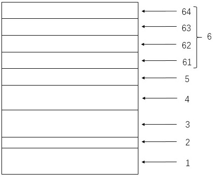
[0043] 3) On the unintentionally doped nitride layer, grow a 2.5 μm N-type nitride layer at a temperature of 1060 °C and a growth pressure of 200 torr, wher...


PUM

PropertyMeasurementUnit
melting pointaaaaaaaaaa

Abstract

The present application provides an organomagnesium compound, which has a structure represented by the following structural formula (1): Structural formula (1) The organomagnesium compound is in a liquid state under working conditions, has a stable high saturated vapor pressure, and is very suitable for semiconductor doping Magnesium source dopant; in the magnesium source process, the magnesium components are evenly distributed, which improves the epitaxy uniformity and production process stability, and is suitable for large-scale substrate epitaxy; on the other hand, the vapor pressure at the end of the magnesium source is also very stable, Therefore, the use efficiency and production efficiency are improved, the production cost is reduced, and it is suitable for mass production.

Description

technical field [0001] The present application relates to the field of metal organic compounds, in particular to an organomagnesium compound and an electronic device. Background technique [0002] The third-generation semiconductor materials are mainly gallium nitride and silicon carbide. The production process is divided into three major steps: single crystal growth, epitaxial layer growth and device manufacturing, corresponding to the industrial chain substrate, epitaxy, devices and modules. links. [0003] Epitaxy is the core intermediate link of the entire industrial chain. The epitaxy process technology directly affects the performance of the device and plays a very critical role in the development of the industry. The metal organic compound is the key supporting raw material for the epitaxy technology. The purity and vapor pressure of the metal organic compound The stability directly determines the performance of the device, so the technical development of metal organ...

Claims


Application Information

Patent Timeline
Patent Type & Authority Patents(China)
IPC IPC(8): C07F3/02H01L33/32
CPCC07F3/02H01L33/325
Inventor 杨敏徐耀中范光华李芳芳刘子伟徐涛沈波
Owner JIANGSU NATA OPTO ELECTRONICS MATERIAL
Why Eureka
Try Eureka