PCB design method for automatically generating MeshLine

A technology of automatic generation and design method, applied in CAD circuit design, computer-aided design, calculation and other directions, can solve the problems of MeshLine being unable to reach the limit tight state, easy to produce artificial differences, long time period, etc., to reduce workload and work. The effect of time, high degree of automation, and high encryption strength

Pending Publication Date: 2021-07-27
EMDOOR ELECTRONICS TECH
View PDF9 Cites 0 Cited by
  • Summary
  • Abstract
  • Description
  • Claims
  • Application Information

AI Technical Summary

Problems solved by technology

[0004] However, in the existing PCB design, the setting of MeshLine needs to be manually set by the PCB designer. The designer needs to design or calculate the relevant parameters according to the demand, and perform related operations in the PCB design software. In this way, the time required for the design The cycle is long, usually one-layer PCB design takes 1-2 working days for a standard PCB engineer, and the time required for the design largely depends on the size of the PCB, and the design time is proportional to the size of the PCB
In addition, since the MeshLine is manually designed by the designer, the degree of density of the MeshLine and the degree of encryption that can be achieved vary from person to person, which is prone to artificial differences, and the number of design layers will be artificially limited, and the MeshLine cannot reach the extreme compact state

Method used


Image

  • PCB design method for automatically generating MeshLine
  • PCB design method for automatically generating MeshLine
  • PCB design method for automatically generating MeshLine

Examples


Embodiment Construction

[0030] In order to make the technical problems, technical solutions and beneficial effects to be solved by the present invention, the present invention will be described in further detail below with reference to the accompanying drawings and examples. It will be appreciated that the specific embodiments described herein are intended to explain the present invention and is not intended to limit the invention.

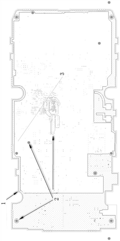
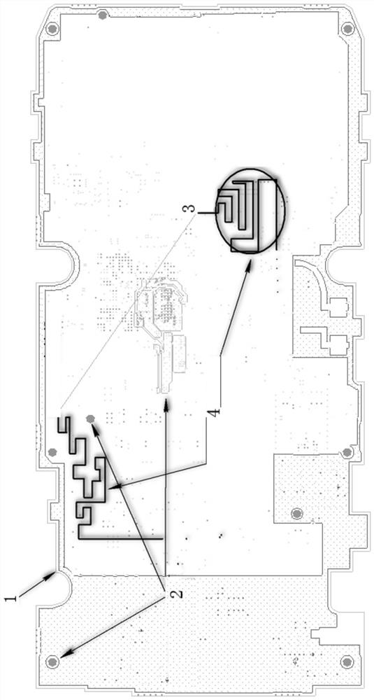
[0031] A PCB design method that automatically generates Meshline, the process is:

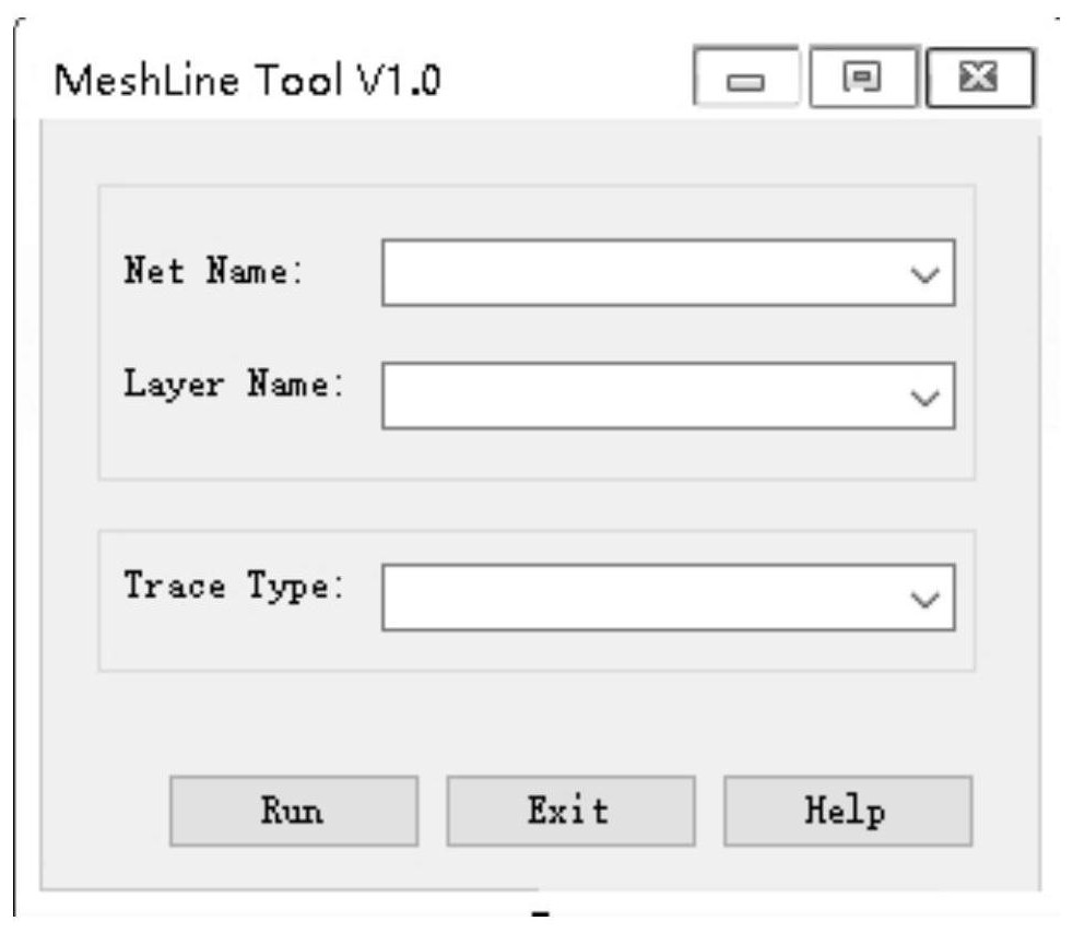
[0032]Step S1. Sign up in the PCB Design Software Automatic Generation Tool, get the PCB information and the meshline design information, and combine the PCB information to extract the Meshline wiring information with the meshline design information.

[0033] MESHLINE Auto Generate Tool Settings Read the PCB Information Program Module, User Enter Program Module, Model Conversion Program Module and Process Communication Module, read PCB Information Program Modules from PCB Information in PCB F...


PUM


Abstract

The invention discloses a PCB design method for automatically generating a MeshLine, which comprises the following steps of: registering a MeshLine automatic generation tool in PCB design software, reading a PCB file by the MeshLine automatic generation tool to obtain PCB information, obtaining MeshLine design information through a MeshLine man-machine interaction interface to form a MeshLine network wiring prohibition area and a MeshLine network wiring available area, and importing the MeshLine design information and the information of the MeshLine network wiring prohibited area and the MeshLine network wiring available area into a mathematical model to form a MeshLine data function expression, thereby completing the MeshLine routing design, reducing the workload of designers, improving the design efficiency, enabling the designed MeshLine routing to have consistency, and enhancing the secrecy degree of the MeshLine.

Description

Technical field [0001] The present invention relates to the field of PCB design, and more particularly, to a PCB design method that automatically generates Meshline. Background technique [0002] Multiple sensitive or confidential data in existing electronic devices, such data should be kept secret, but since electronic devices are multi-PCB-bearing basis, special processing or special equipment is usually processed on the PCB. Protection of such data to protect and conceal relevant data. [0003] In the existing PCB design, in order to prevent others from illegally extracting or stealing data of electronic devices, there is usually a walking line called meshline (grid line) on the PCB. Meshline is a physical security protection mechanism for PCI DSS (PCI, PAYMENT CARDUSTRY DATA Security Standard, third-party payment industry data security standard) for protecting handheld electronic devices such as POS or sensitive devices. Once these devices are opened or subject to external de...

Claims


Application Information

Patent Timeline
Patent Type & Authority Applications(China)
IPC IPC(8): G06F30/398G06F30/394G06F115/12
CPCG06F30/398G06F30/394G06F2115/12
Inventor 明睿王灿钟
Owner EMDOOR ELECTRONICS TECH
Why Eureka
Try Eureka