Electronic device processing system

A processing system and electronic device technology, applied in metal processing, etc., can solve problems affecting work efficiency, inability to install heat-conducting silicone pads, long processing time, etc.

Inactive Publication Date: 2021-03-30
HARBIN UNIV
View PDF1 Cites 1 Cited by
  • Summary
  • Abstract
  • Description
  • Claims
  • Application Information

AI Technical Summary

Problems solved by technology

It relates to the field of optoelectronic devices. The integrated optoelectronic device processing equipment is equipped with a box body, a baffle body and a dust collection tank, and the vertical section of the baffle body is trapezoidal in shape. And the effect of preventing dust from scattering, thus effectively solving the problem that the dust removal of general integrated optoelectronic device processing equipment is not convenient, the processing time is long, and the work efficiency is affected to a certain extent; but the device cannot be installed on the electronic device Thermal Silicone Pad

Method used


Image

  • Electronic device processing system
  • Electronic device processing system
  • Electronic device processing system

Examples


specific Embodiment approach 1

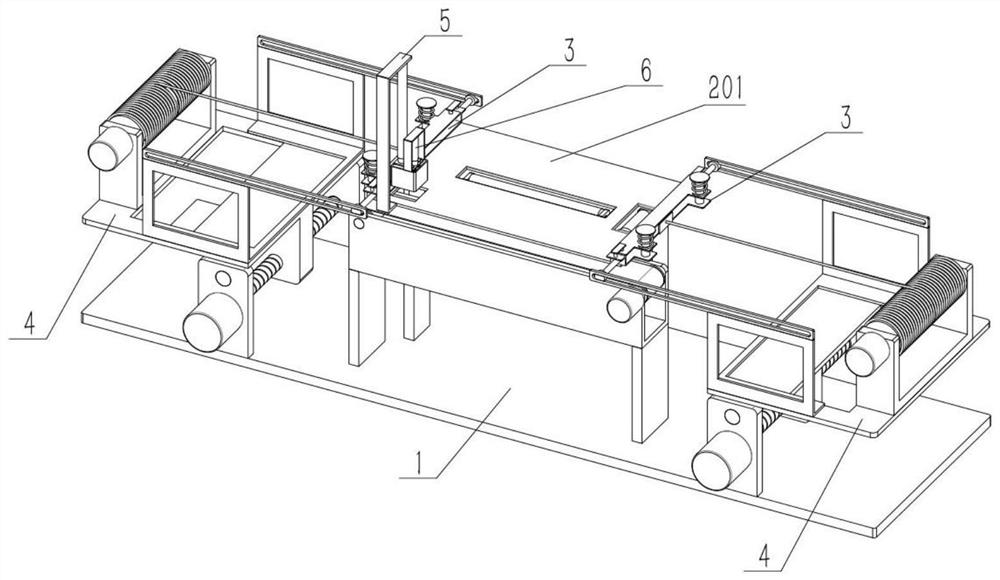
[0029] As shown in the figure, an electronic device processing system includes a bracket I5, an electric push rod II501, a cutter 502, a bracket II503, an electric push rod III6 and a push plate 603, and the upper end of the bracket I5 is fixedly connected to the electric push rod II501, The cutter 502 is fixedly connected to the movable end below the electric push rod II 501, the upper end of the cutter 502 is fixed to the bracket II 503, the electric push rod III6 is fixed to the bracket II 503, the push plate 603 is arranged under the electric push rod III 6, and the electric push rod III The rod III6 is used to drive the push plate 603 up and down, and the push plate 603 is located inside the cutter 502 . Set the silicone heat conduction pad used for electronic devices under the cutter 502, start the electric push rod II 501, the electric push rod II 501 and the electric cutter 502 descend, and the cutter 502 cuts off a piece of the silicone heat conduction pad. The cutter ...

specific Embodiment approach 2

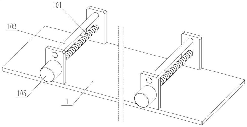
[0031] As shown in the figure, the electronic device processing system also includes a mounting plate 601 and a vertical rod II 602. The movable end of the electric push rod III6 is fixed to the mounting plate 601, and the mounting plate 601 is slidably connected to two vertical rods II 602 and a push plate 603. It is fixedly connected to the lower ends of the two vertical rods II602, and the upper ends of the two vertical rods II602 are fixedly connected to the limit piece. A compression spring, the two ends of the compression spring are in contact with the mounting plate 601 and the push plate 603 respectively. Use the compression spring to make the force generated by the push plate 603 when pressing the silicone heat conduction pad on the electronic device change from small to large, and simulate pressing to avoid the electronic device from being crushed, so that the precision required for the installation of the silicone heat conduction pad is reduced, and excessive pressur...

specific Embodiment approach 3

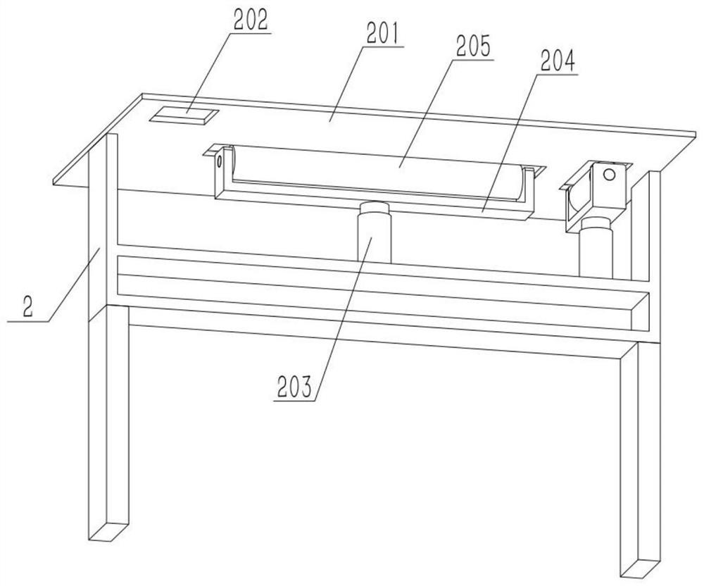
[0033] As shown in the figure, the electronic device processing system also includes a table support 2 , a desktop 201 and a cutout 202 , the upper end of the table support 2 is fixed to the desktop 201 , and the left rear corner of the desktop 201 is provided with a cutout 202 . Place the silicone heat conduction pad on the desktop 201, and the cutout 202 is used to allow the cutter 502 to pass through, and then support the silicone pad through the desktop 201. When the cutter 502 cuts the silicone pad through the cutout 202, the cut part of the silicone pad can be better. Good stretching is conducive to extrusion into the cutter 502, and the lower edge of the cutter 502 is sharp.


PUM


Abstract

The invention relates to electrical device processing, in particular to an electronic device processing system. The electronic device processing system comprises a support I, an electric push rod II,a cutter, a support II, an electric push rod III and a push plate; the upper end of the support I is fixedly connected with the electric push rod II; the cutter is fixedly connected to the movable endbelow the electric push rod II; the upper end of the cutter is fixedly connected with the support II; the electric push rod III is fixedly connected to the support II; the push plate is arranged below an electric push rod III; and the electric push rod III is used for driving the push plate to lift, and the push plate is located in the cutter. The cutter is of a surrounding structure, openings are formed in the upper end and the lower end of the cutter, and the cutter can be of structures of different shapes and sizes such as squares or circles so as to be suitable for electronic devices of different shapes or specifications. Due to the fact that a silica gel heat-conducting pad is flexible, when the cutter descends to cut the heat-conducting pad, the heat-conducting pad is deformed and stretched downward, and then squeezed into the cutter, then the heat-conducting pad is extruded into the cutter, so that the cutter continues to descend to penetrate through the heat-conducting pad, andan electronic device is arranged below the heat-conducting pad, the cutter can drive the heat-conducting pad to be directly close to the electronic device, and the installation stroke of the heat-conducting pad is shortened.

Description

technical field [0001] The invention relates to electrical device processing, more specifically an electronic device processing system. Background technique [0002] For example, the publication number is CN208542618U, a kind of integrated optoelectronic device processing equipment, including a box body and a transmission belt. The surface of the box body is provided with an inlet, the surface of the box body is provided with an outlet, and the surface of the transmission belt is movably connected with an electronic device circuit board. There is a cavity inside the box body, the inner wall of the box body is fixedly connected with a support plate, the surface of the support plate is provided with a baffle body, the surface of the baffle body and the surface of the support plate are fixedly connected with a suction pipe, and one end of the suction pipe It is in fixed communication with the inner wall of the cavity. It relates to the field of optoelectronic devices. The inte...

Claims


Application Information

Patent Timeline
IPC IPC(8): B26F1/40B26D7/02
CPCB26D7/025B26F1/40
Inventor 郭丽华
Owner HARBIN UNIV
Why Eureka
Try Eureka