Eureka AIR delivers breakthrough ideas for toughest innovation challenges, trusted by R&D personnel around the world.

Photoelectric chip packaging structure and packaging method thereof

A packaging structure, optoelectronic chip technology, applied in the direction of light guide, optics, optical components, etc., to achieve the effect of improving reliability, not easy to warp, and improving performance

Active Publication Date: 2020-12-04
NAT CENT FOR ADVANCED PACKAGING
View PDF4 Cites 8 Cited by
  • Summary
  • Abstract
  • Description
  • Claims
  • Application Information

AI Technical Summary

Problems solved by technology

[0005] Therefore, the technical problem to be solved by the present invention is to overcome how to simultaneously improve packaging reliability and reduce light leakage in the prior art

Method used


Image

  • Photoelectric chip packaging structure and packaging method thereof
  • Photoelectric chip packaging structure and packaging method thereof
  • Photoelectric chip packaging structure and packaging method thereof

Examples


Embodiment Construction

[0035] As mentioned in the background, the performance of the existing optoelectronic chip packaging structure is relatively poor.

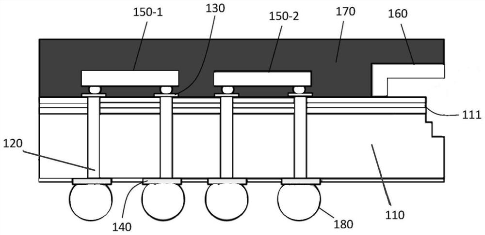
[0036] An optoelectronic chip packaging structure, such as figure 1 , including: an optical chip, the optical chip includes an optical core semiconductor substrate 110 and an optical interconnection structure 111; an electrical chip 150 (150-1, 150-2); a cover plate 160; a plastic sealing layer 170; a conductive connector 120; A wiring layer 130 ; a second wiring layer 140 ; ​​solder balls 180 .

[0037]In the above optoelectronic chip packaging structure, one side of the optical interconnection structure 111 has an optical coupling area, and a mode spot converter is provided in the optical optical coupling area. The material of the cover plate 160 is usually glass, and the cover plate 160 is not in contact with the optical coupling area. , but the gap between the cover plate 160 and the optical coupling region forms a cavity. There is a cavity...


PUM

PropertyMeasurementUnit
thicknessaaaaaaaaaa
thicknessaaaaaaaaaa
refractive indexaaaaaaaaaa

Abstract

The invention discloses a photoelectric chip packaging structure and a packaging method thereof. The photoelectric chip packaging structure comprises an optical chip and a protection structure; the optical chip comprises an optical dielectric layer; the edge region of one side of the optical dielectric layer is an optical coupling region; the protection structure is located on the front face of the optical chip and makes contact with the surface of the optical coupling region; the refractive index of the protection structure is smaller than that of the optical medium layer. The packaging reliability of the photoelectric chip packaging structure is improved, and light leakage is reduced.

Description

technical field [0001] The invention relates to the packaging field, in particular to a photoelectric chip packaging structure and a packaging method thereof. Background technique [0002] Optical communication is a communication method in which light waves are used as carriers. With the development of technology, the amount of communication data is getting larger and larger, so the requirements for the transmission rate of optical communication modules are getting higher and higher. The photoelectric chip integrated structure is the core component of the optical communication module. The result of photoelectric chip integration is to integrate the optical chip and the electrical chip of its peripheral circuit to realize the function of converting between optical signal and electrical signal. [0003] One edge of the optical chip has an optical coupling area, and there is generally a spot converter in the optical coupling area. One end of the spot converter has a larger sp...

Claims


Application Information

Patent Timeline
Patent Type & Authority Applications(China)
IPC IPC(8): G02B6/42G02B6/12G02B6/14
CPCG02B6/4204G02B6/4243G02B6/4249G02B6/4274G02B6/12G02B6/14G02B2006/12038G02B2006/12061G02B2006/12138G02B2006/12142G02B2006/12152
Inventor 王全龙曹立强严阳阳戴风伟
Owner NAT CENT FOR ADVANCED PACKAGING
Why Eureka
Eureka Blog
Learn More