
variable gate transistor

A transistor and variant technology, applied in the field of CMOS transistor layout, can solve the problems of edge leakage current and ring gate area consumption of common gate transistors, asymmetry of source and drain regions, etc.

Active Publication Date: 2014-04-30
SHANGHAI FUDAN MICROELECTRONICS GROUP
View PDF0 Cites 1 Cited by
  • Summary
  • Abstract
  • Description
  • Claims
  • Application Information

AI Technical Summary

Problems solved by technology

[0004] The problem to be solved by the present invention is to eliminate the edge leakage current of ordinary gate transistors and the large consumption of ring gate area, and the source and drain regions are asymmetrical. The present invention proposes a variable gate transistor that can be applied in radiation-resistant layout reinforcement technology

Method used


Image

  • variable gate transistor
  • variable gate transistor
  • variable gate transistor

Examples


Embodiment Construction

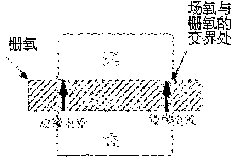
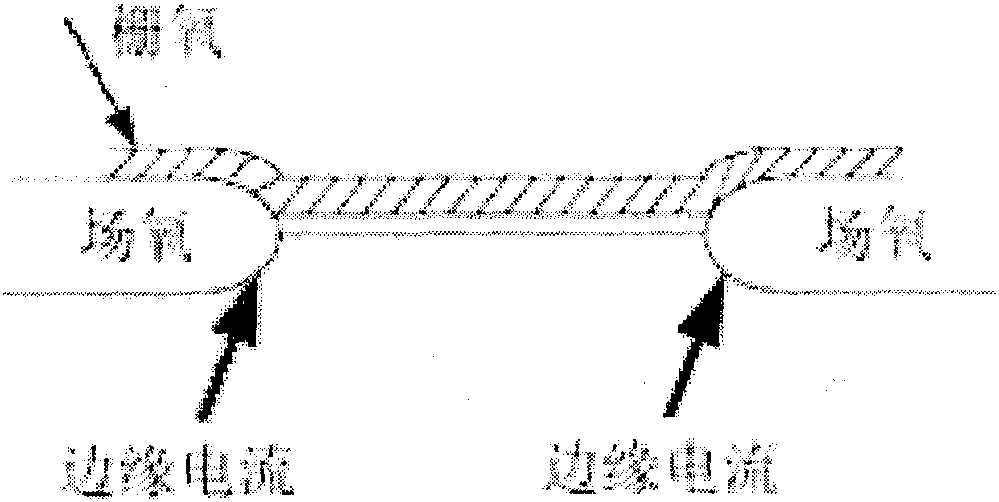
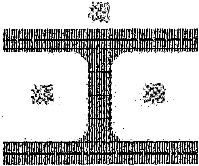
[0019] As shown in Figure 1 and Figure 2, this structure is a state-of-the-art structure diagram, the gate straddles the transistor channel, and overlaps with the field oxygen edge as field isolation at the edge of the transistor, and the source region and the drain are respectively on both sides Area. When no bias is applied to the gate, no inversion layer is formed under the gate oxide, and the transistor is turned off. Apply a bias voltage that is appropriately greater than the threshold voltage on the gate, an inversion layer is formed under the gate oxide, and there is a conductive channel. When an appropriate bias voltage is applied to both ends of the source and drain, current will flow, and the voltage and current characteristics exhibited are very good. Realize the transistor function. Such as image 3 As shown, the gate straddles the channel of the transistor, the two sides are the source region and the drain region, and the gate is used to cover the edge of the act...


PUM


Abstract

The invention proposes a variable gate transistor that can be applied in the anti-radiation layout reinforcement technology. Including inserting gate oxide between the source terminal and the source terminal edge, between the drain terminal and the drain terminal edge, thereby cutting off the path from the source terminal to the source terminal edge and cutting off the current from the source terminal to the source terminal edge to the drain terminal edge to the drain terminal , while cutting off the current from drain to drain edge to source edge to source. Using this method, the basic structure of the transistor does not change, and the edge leakage current is well eliminated. Compared with ordinary gate transistors, for the same effective width-to-length ratio, the variable-gate transistor does not increase the area, and the effective width-to-length ratio is basically the same as that of ordinary gate transistors. The gate is consistent, and the source and drain regions are completely symmetrical.

Description

technical field [0001] The invention relates to the technical field of CMOS transistor layout, in particular to a variable gate transistor which can be applied in radiation-resistant layout reinforcement technology. Background technique [0002] In the current CMOS transistor layout technology, the transistor adopts a common shape gate structure. As shown in Fig. 1 and Fig. 2, in this structure, the gate straddles the channel of the transistor, and overlaps the edge of the field oxygen as field isolation at the edge of the transistor, and the two sides are the source region and the drain region respectively. When no bias is applied to the gate, no inversion layer is formed under the gate oxide, and the transistor is turned off. Apply a bias voltage that is appropriately greater than the threshold voltage on the gate, an inversion layer is formed under the gate oxide, and a conductive channel exists, and current will flow through an appropriate bias voltage at both ends of t...

Claims


Application Information

Patent Timeline
Patent Type & Authority Patents(China)
IPC IPC(8): H01L21/8238
Inventor 沈鸣杰俞剑华霞俞军
Owner SHANGHAI FUDAN MICROELECTRONICS GROUP
Learn More