


Quick Research
Generate reliable direction feasibility study reports for your R&D in just a few steps.

Technical Q&A
Discover and master advanced knowledge NOW. Basics, ideas, possibilities, all at once.

Find Solutions
As an expert in R&D theories, this can generate solutions to your technical problems instantly.

Evaluate Feasibility
Analyze your overall solution with one click, know your potential R&D risks in advance.

Monitor Landscape
Get weekly tech updates, stay abreast of the latest tech innovations and key insights.
Display substrate, display device and manufacturing method thereof
A display substrate and manufacturing method technology, applied in identification devices, organic semiconductor devices, instruments, etc., can solve problems such as box thickness, light leakage, and affecting display effects
- Summary
- Abstract
- Description
- Claims
- Application Information
AI Technical Summary
Problems solved by technology
Method used
Image

Examples
Embodiment 1
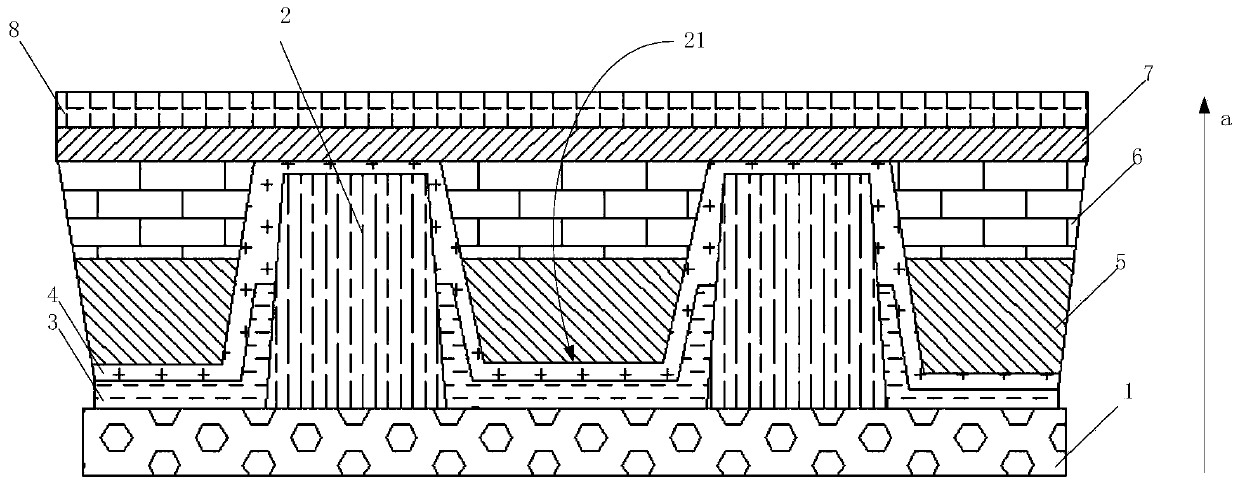
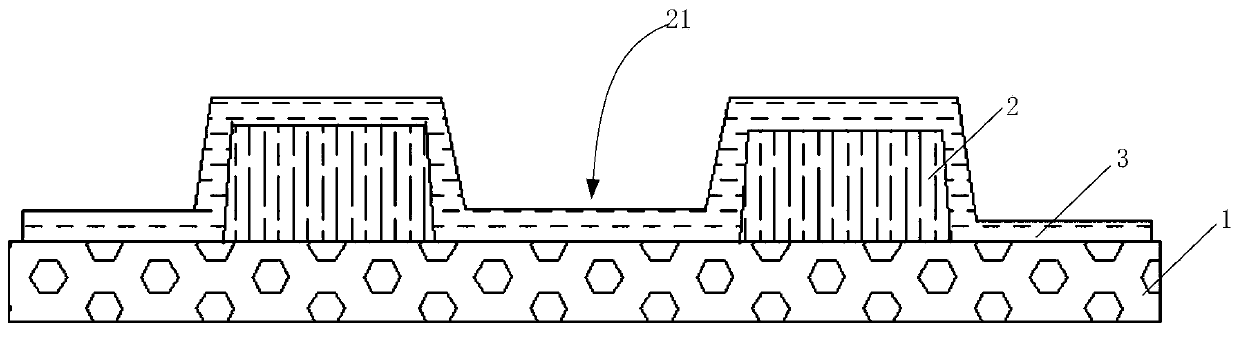
[0041] Reference attached figure 1 , the display substrate provided by the embodiment of the present invention, which includes a TFT substrate 1, a pixel defining layer 2, an electroluminescent device layer 3, a connection layer 4, a first encapsulation layer 5, and a quantum dot layer 6; the pixel defining layer 2 is set On the TFT substrate 1, and surround several pixel pits 21;
[0042] Each of the pixel pits 21 is sequentially stacked with an electroluminescent device layer 3, a connection layer 4, a first encapsulation layer 5, and a quantum dot layer 6, and the connection layer 4 in the adjacent pixel pit 21 is The side of the pixel defining layer 2 that is away from the TFT substrate 1 is in contact with each other, and is used for electrically connecting the electroluminescent device layers 3 in two adjacent pixel pits 21 .
[0043] Specifically, in order to solve the problem that when quantum dots are applied in flexible OLED display devices, the conventional box-ali...
Embodiment 2
[0063] Further, an embodiment of the present invention provides a display device, which includes the display substrate described in the above embodiments.
[0064] It can be understood that, the display substrate in this embodiment can directly use the display substrate described in Embodiment 1, and its detailed structure can refer to the content of the above embodiment.
Embodiment 3
[0066] Reference attached Figure 4 , an embodiment of the present invention provides a method for manufacturing a display substrate based on Embodiment 1, which includes the following steps:
[0067] 101. Making a TFT substrate 1;
[0068] Specifically, it is not difficult for those skilled in the art to fabricate a thin film transistor (TFT) circuit on a base substrate according to the conventional technology, so details will not be repeated here.
[0069] 102. Fabricate a pixel defining layer 2 on the TFT substrate 1, and surround several pixel pits 21;
[0070] Specifically, a directional thermal expansion material is selected as the pixel defining layer 2, and the pixel defining layer 2 is fabricated on the TFT substrate 1 by inkjet printing, and several pixel pits 21 are formed.
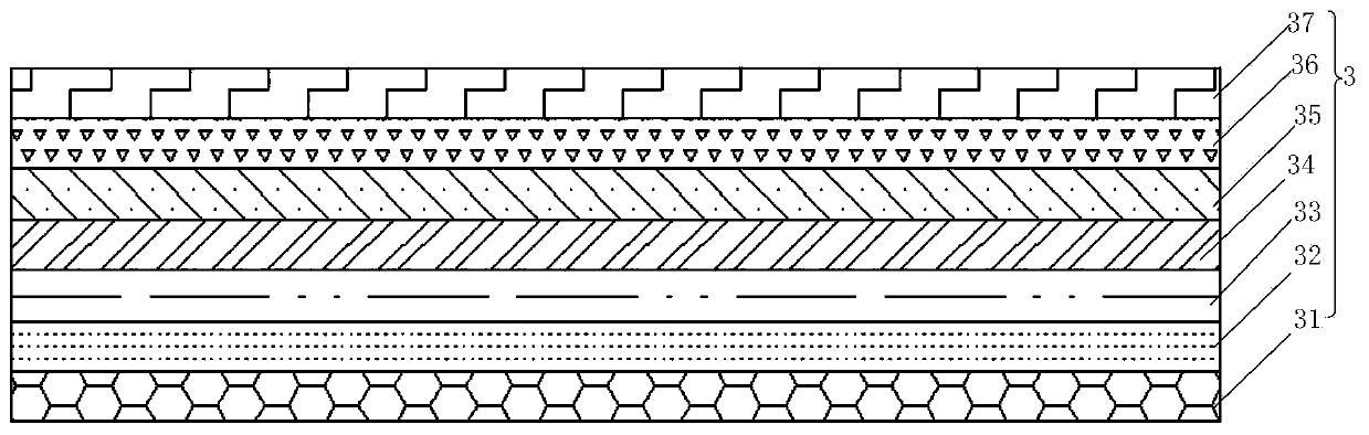
[0071] 103. Arranging an electroluminescent device layer 3 on the side of the pixel defining layer 2 away from the TFT substrate 1;
[0072] Specifically, the electroluminescent device layer...
PUM
| Property | Measurement | Unit |
|---|---|---|
| Particle size | aaaaa | aaaaa |
Abstract
Description
Claims
Application Information
 - R&D Engineer
- R&D Manager
- IP Professional
- Industry Leading Data Capabilities
- Powerful AI technology
- Patent DNA Extraction
Browse by: Latest US Patents, China's latest patents, Technical Efficacy Thesaurus, Application Domain, Technology Topic, Popular Technical Reports.
© 2024 PatSnap. All rights reserved.Legal|Privacy policy|Modern Slavery Act Transparency Statement|Sitemap|About US| Contact US: help@patsnap.com