An emission optical power monitoring device and its preparation method
A monitoring device and technology for emitting light, applied in the field of optical communication, can solve the problem that the monitoring scheme of emitted light power cannot be applied to optical module products, etc., and achieve the effect of reliable optical power monitoring
- Summary
- Abstract
- Description
- Claims
- Application Information
AI Technical Summary
Problems solved by technology
Method used
Image

Examples
Embodiment 1
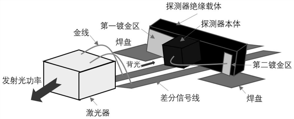
[0035] This embodiment provides a device for monitoring emitted light power, including: a laser, a detector body, a detector insulating carrier, and a PCB.
[0036] Such as image 3 As shown, the PCB is provided with differential signal lines (ie image 3 The two thin and long PCB traces in), the pad (ie image 3 two square PCB traces), the pads are located on both sides of the differential signal line. The laser is connected to the laser driver through the differential signal line.
[0037] The detector insulating carrier is disposed between the laser and the laser driver, and the first surface of the detector insulating carrier is in contact with the PCB.
[0038] Since the first surface of the detector insulating carrier close to the differential signal line is non-conductive, the detector insulating carrier will not affect the signal quality of the differential signal line. In addition, the upper surface of the differential signal line is covered with green oil, which ...
Embodiment 2
[0049] An emission optical power monitoring device provided in Embodiment 2 includes N monitoring units, each of which includes one of the lasers, one of the detector bodies, and one of the detector insulating carriers, and N of the monitoring units The units share one said PCB.
[0050] In one design solution, 2N pads are provided on the PCB.
[0051] In another design solution, part of the pads may be shared between some adjacent monitoring units. For example, if a device for monitoring optical power includes four monitoring units (respectively denoted as the first road, the second road, the third road, and the fourth road), then only six solder pads can be arranged on the PCB. , one pad can be shared between the first and second monitoring units, and one pad can be shared between the third and fourth monitoring units.
[0052] The following takes the 100G CWDM4 optical module as an example to describe the transmitting optical power monitoring device.
[0053] Since the 1...
Embodiment 3
[0061] Embodiment 3 provides the preparation method of the above-mentioned emission optical power monitoring device (emission optical power monitoring device in embodiment 1 or embodiment 2), which mainly includes the following steps:
[0062] Step 1. Preset pads and differential signal lines on the PCB;
[0063] Step 2, attaching the insulating carrier of the detector to the PCB, and connecting the pad of the PCB with the gold-plated area of the insulating carrier of the detector through conductive silver glue;
[0064] Step 3, attaching the detector body to the detector insulating carrier, and electrically connecting the detector body and the gold-plated area of the detector insulating carrier;
[0065] Step 4, mounting a laser on the PCB, and connecting the laser to the differential signal line through a gold wire.
[0066] Taking the 100G CWDM4 optical module as an example, the preparation method of the emission optical power monitoring device includes the following s...
PUM
 Abstract
Description
Claims
Application Information
 - R&D
- Intellectual Property
- Life Sciences
- Materials
- Tech Scout
- Unparalleled Data Quality
- Higher Quality Content
- 60% Fewer Hallucinations
Browse by: Latest US Patents, China's latest patents, Technical Efficacy Thesaurus, Application Domain, Technology Topic, Popular Technical Reports.
© 2025 PatSnap. All rights reserved.Legal|Privacy policy|Modern Slavery Act Transparency Statement|Sitemap|About US| Contact US: help@patsnap.com