
A transistor equivalent transconductance boosting amplifier circuit and chip

An amplifier circuit and transistor technology, applied in power amplifiers and other directions, can solve the problems of limited application range and low gain of MO-TFT amplifier, and achieve the effect of improving circuit stability and increasing gain.

Active Publication Date: 2021-01-05
SOUTH CHINA UNIV OF TECH
View PDF5 Cites 0 Cited by
  • Summary
  • Abstract
  • Description
  • Claims
  • Application Information

AI Technical Summary

Problems solved by technology

Due to the lack of p-type devices as current mirror loads, MO-TFT amplifiers have low gain, usually below 30dB, which limits their application range

Method used


Image

  • A transistor equivalent transconductance boosting amplifier circuit and chip
  • A transistor equivalent transconductance boosting amplifier circuit and chip
  • A transistor equivalent transconductance boosting amplifier circuit and chip

Examples


Embodiment 1

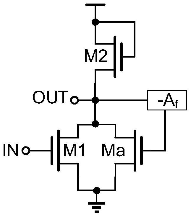
[0028] refer to figure 1 , a transistor equivalent transconductance improvement amplifier circuit, including a drive transistor M1, a load transistor M2, a feedback network-Af and an auxiliary transistor Ma, the power supply is connected to the drain and gate of the load transistor M2, and the gate of the drive transistor M1 is connected to the input Terminal IN, the source of the driving transistor M1 and the source of the auxiliary transistor Ma are connected to the common ground, the source of the load transistor M2 is connected to the drain of the driving transistor M1 and the drain of the auxiliary transistor Ma, and the gate of the auxiliary transistor Ma passes through the feedback network -Af is connected to the source of the load transistor M2 and the output terminal OUT.

[0029] When the input signal increases, the current flowing through the load transistor M2 increases, and then the output signal decreases, which causes the gate voltage of the auxiliary transistor...

Embodiment 2

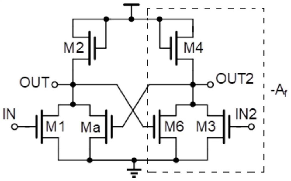
[0038] refer to Figure 2-4 , on the basis of Embodiment 1, the feedback network-Af includes a second drive transistor M3, a second load transistor M4, a second auxiliary transistor M6, the power supply is connected to the drain and gate of the second load transistor M4, and the second drive transistor The gate of M3 is connected to the second input terminal IN2, the source of the second driving transistor M3 and the source of the second auxiliary transistor M6 are connected to the common ground, and the source of the second load transistor M4 is connected to the drain of the second driving transistor M3 and The drain of the second auxiliary transistor M6, the gate of the auxiliary transistor Ma are connected to the source of the second load transistor M4 and the second output terminal OUT2, the gate of the second auxiliary transistor M6 is connected to the source of the load transistor M2. The voltage between the second input terminal IN2 and the input terminal IN of the feed...

Embodiment 3

[0050] A transistor equivalent transconductance improvement amplifier chip, the chip includes the circuit of embodiment 1 or the circuit of embodiment 2.


PUM


Abstract

The invention discloses a transistor equivalent transconductance improving amplifier circuit, and relates to an amplification circuit. The technical problem that an existing amplifier is low in gain is mainly solved. The circuit comprises a driving transistor, a load transistor, a feedback network and an auxiliary transistor, the power supply is connected with the drain electrode and the grid electrode of the load transistor. The grid electrode of the driving transistor is connected with the input end; the source electrode of the driving transistor and the source electrode of the auxiliary transistor are in common-ground connection, the source electrode of the load transistor is connected with the drain electrode of the driving transistor and the drain electrode of the auxiliary transistor, and the grid electrode of the auxiliary transistor is connected with the source electrode and the output end of the load transistor through the feedback network. The invention further discloses a transistor equivalent transconductance improving amplifier chip. The gain can be effectively improved.

Description

technical field [0001] The invention relates to an amplifier circuit, more specifically, it relates to a transistor equivalent transconductance-improving amplifier circuit and a chip. Background technique [0002] Metal-oxide-semiconductor thin-film transistors (MO-TFTs) have attracted extensive attention due to their high carrier mobility, good uniformity, low process temperature, and compatibility with flexible and transparent electronic applications. In recent years, the design of MO-TFT integrated circuits has attracted more and more researchers' interest, and it is a hot research direction. However, due to the lack of high-performance complementary (p-type) devices, most MO-TFT circuits can only be realized using pure n-type devices. [0003] Amplifiers are important building blocks in circuits such as biopotential measurement front ends, data converters, DC-DC converters, and sensor systems. Due to the lack of p-type devices as current mirror loads, MO-TFT amplifiers...

Claims


Application Information

Patent Timeline
Patent Type & Authority Patents(China)
IPC IPC(8): H03F3/20
CPCH03F3/20
Inventor 徐煜明陈荣盛吴朝晖李斌
Owner SOUTH CHINA UNIV OF TECH
Learn More