Gas distributors and semiconductor equipment in semiconductor equipment

A gas distributor and gas distribution technology, applied in the direction of gaseous chemical plating, metal material coating process, coating, etc., can solve the problems of pipeline residue, edge thickness, poor film thickness uniformity, etc., to improve service life, convenient Cleaning, improving uniformity

Active Publication Date: 2022-07-22
BEIJING NAURA MICROELECTRONICS EQUIP CO LTD
View PDF0 Cites 0 Cited by
  • Summary
  • Abstract
  • Description
  • Claims
  • Application Information

AI Technical Summary

Problems solved by technology

Among them, for NH 3 , O 2 , Ar and N 2 and other reaction sources, can realize rapid transmission and purging; however, for more viscous, easy to condense and difficult to purify 2 O, TMA, TiCl 4 , PDMAT, etc., are very easy to remain in the pipeline, so that chemical vapor deposition occurs around the gas outlet of the gas outlet pipeline to form a film, which in turn leads to the phenomenon that the deposited film on the substrate is thin in the middle and thick at the edge
image 3 is a schematic diagram of the thickness distribution of a thin film deposited based on an existing gas distributor, from image 3 It can be seen that the thickness uniformity of the film is poor

Method used


Image

  • Gas distributors and semiconductor equipment in semiconductor equipment
  • Gas distributors and semiconductor equipment in semiconductor equipment
  • Gas distributors and semiconductor equipment in semiconductor equipment

Examples


Embodiment Construction

[0029] The specific embodiments of the present invention will be described in detail below with reference to the accompanying drawings. It should be understood that the specific embodiments described herein are only used to illustrate and explain the present invention, but not to limit the present invention.

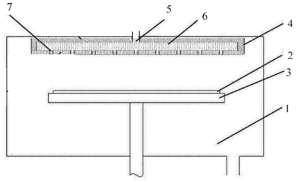
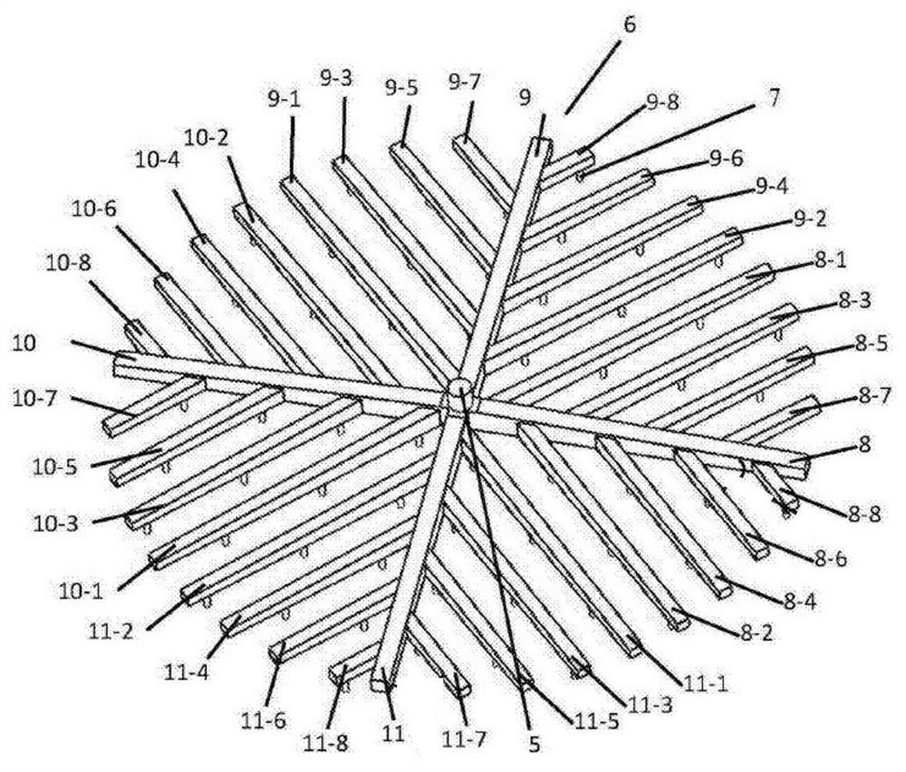
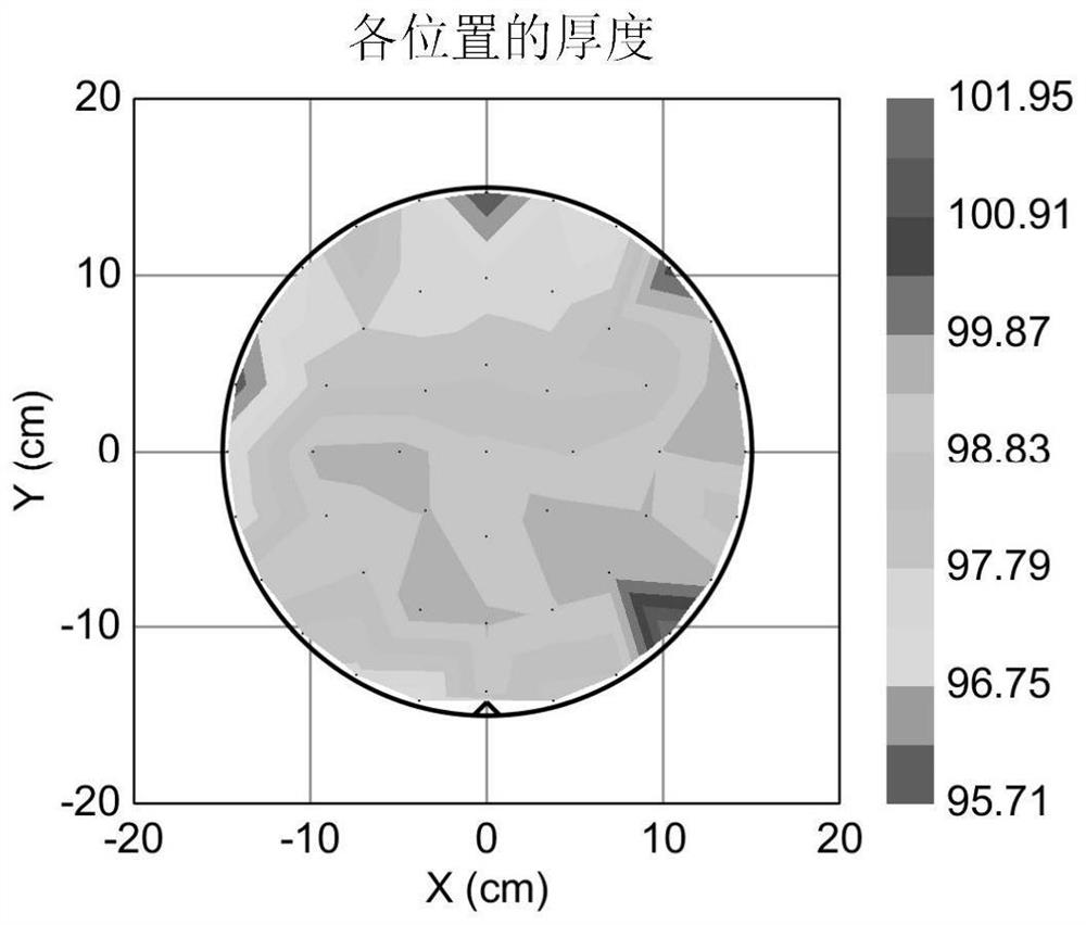
[0030] In a first aspect, an embodiment of the present invention provides a gas distributor in a semiconductor device. Optionally, the semiconductor device is a thin film deposition device. Figure 4 It is a top view of the gas distributor provided in the embodiment of the present invention, Figure 5 for the edge Figure 4 Sectional view of the middle AA' line, Image 6 for the edge Figure 4 Sectional view of the middle BB' line, combined with Figure 4 to Figure 6 As shown, the gas distributor includes a distributor main body 110, the distributor main body 110 has a gas outlet end face 111, and the distributor main body 110 is provided with: a gas distribution pip...


PUM

PropertyMeasurementUnit
heightaaaaaaaaaa
heightaaaaaaaaaa
diameteraaaaaaaaaa

Abstract

The invention provides a gas distributor in a semiconductor device, comprising a distributor main body, and the distributor main body is provided with: a gas distribution pipeline, a first air intake pipeline and a plurality of first air outlet pipelines, and the first air intake pipeline is connected with The air inlets of the gas distribution pipelines are connected, and the plurality of first air outlet pipelines are connected with the plurality of air outlets of the gas distribution pipelines in one-to-one correspondence; the main body of the distributor is also provided with: a gas distribution cavity and a second air inlet pipeline and a plurality of second gas outlet pipelines, the gas distribution cavity is located above the gas distribution pipeline and is arranged around the first intake pipeline, the height of the gas distribution cavity gradually decreases from the middle to the edge, the second intake pipeline and the gas distribution cavity are The air inlets are connected to each other, and the plurality of second air outlet pipelines are in communication with the plurality of air outlets of the gas distribution chamber in one-to-one correspondence. . The present invention also provides a semiconductor device. The present invention can improve the uniformity of thin film deposition.

Description

technical field [0001] The present invention relates to the technical field of semiconductors, in particular to a gas distributor in a semiconductor device and a semiconductor device. Background technique [0002] Atomic layer deposition technology is a thin film preparation technology that is adsorbed layer by layer on a substrate in the form of a single atomic layer. Atomic layer deposition technology mainly includes two reaction processes: the first reaction process is: the first reaction precursor enters the reaction The chamber is fully adsorbed on the substrate, and after reaching the saturation state, the remaining reaction precursors and by-products are removed by the purge gas; the second reaction process is: the second reaction precursor enters the reaction chamber, and is mixed with the existing reaction precursors. The groups adsorbed on the surface of the substrate react to release reaction by-products; after saturated adsorption is formed, the remaining reactio...

Claims


Application Information

Patent Timeline
Patent Type & Authority Patents(China)
IPC IPC(8): C23C16/455
CPCC23C16/45544C23C16/45561C23C16/45574C23C16/45578C23C16/4401
Inventor 赵雷超史小平兰云峰王勇飞秦海丰张文强纪红
Owner BEIJING NAURA MICROELECTRONICS EQUIP CO LTD
Why Eureka
Try Eureka