


Quick Research
Generate reliable direction feasibility study reports for your R&D in just a few steps.

Technical Q&A
Discover and master advanced knowledge NOW. Basics, ideas, possibilities, all at once.

Find Solutions
As an expert in R&D theories, this can generate solutions to your technical problems instantly.

Evaluate Feasibility
Analyze your overall solution with one click, know your potential R&D risks in advance.

Monitor Landscape
Get weekly tech updates, stay abreast of the latest tech innovations and key insights.
Pixel structure, display panel and display device
A pixel structure and display panel technology, applied in static indicators, instruments, semiconductor devices, etc., can solve the problems of increasing module thickness, increasing process cost, reducing the number of ICs used, and achieving the effect of solving the problem of arrangement structure
- Summary
- Abstract
- Description
- Claims
- Application Information
AI Technical Summary
Problems solved by technology
Method used
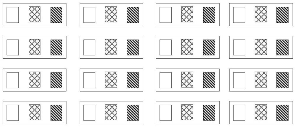
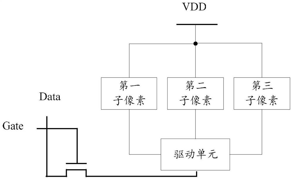
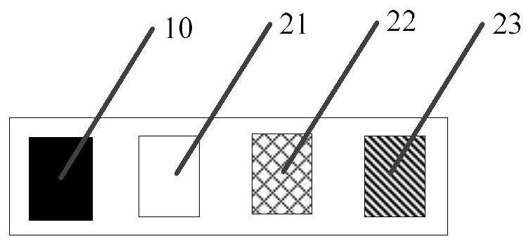
Image

Examples
Embodiment Construction
[0037] The application will be further described in detail below in conjunction with the accompanying drawings and embodiments. It should be understood that the specific embodiments described here are only used to explain related inventions, rather than to limit the invention. It should also be noted that, for ease of description, only parts related to the invention are shown in the drawings.
[0038] Unless otherwise defined, the technical terms or scientific terms used in the present disclosure shall have the usual meanings understood by those skilled in the art to which the present invention belongs. "First", "second" and similar words used in the present disclosure do not indicate any order, quantity or importance, but are only used to distinguish different components. "Comprising" or "comprising" and similar words mean that the elements or items appearing before the word include the elements or items listed after the word and their equivalents, without excluding other el...
PUM
 Abstract
Description
Claims
Application Information
 - R&D Engineer
- R&D Manager
- IP Professional
- Industry Leading Data Capabilities
- Powerful AI technology
- Patent DNA Extraction
Browse by: Latest US Patents, China's latest patents, Technical Efficacy Thesaurus, Application Domain, Technology Topic, Popular Technical Reports.
© 2024 PatSnap. All rights reserved.Legal|Privacy policy|Modern Slavery Act Transparency Statement|Sitemap|About US| Contact US: help@patsnap.com