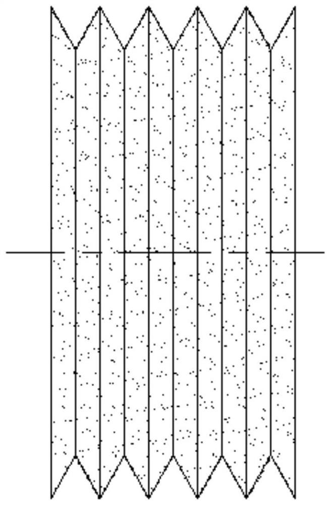
Ceramic insulator with microgrooves and self-assembled molecular film on the surface and preparation method thereof
A ceramic insulator and self-assembly technology, which is applied in the direction of insulators, electrical components, circuits, etc., can solve the problems of insignificant boosting effect of flashover voltage along the vacuum surface, single surface of ceramic insulators, and difficulty in putting into practical application, etc., and achieve good adhesion performance , not easy to fall off, enhance the effect of stability
- Summary
- Abstract
- Description
- Claims
- Application Information
AI Technical Summary
Problems solved by technology
Method used
Image
Examples
preparation example Construction
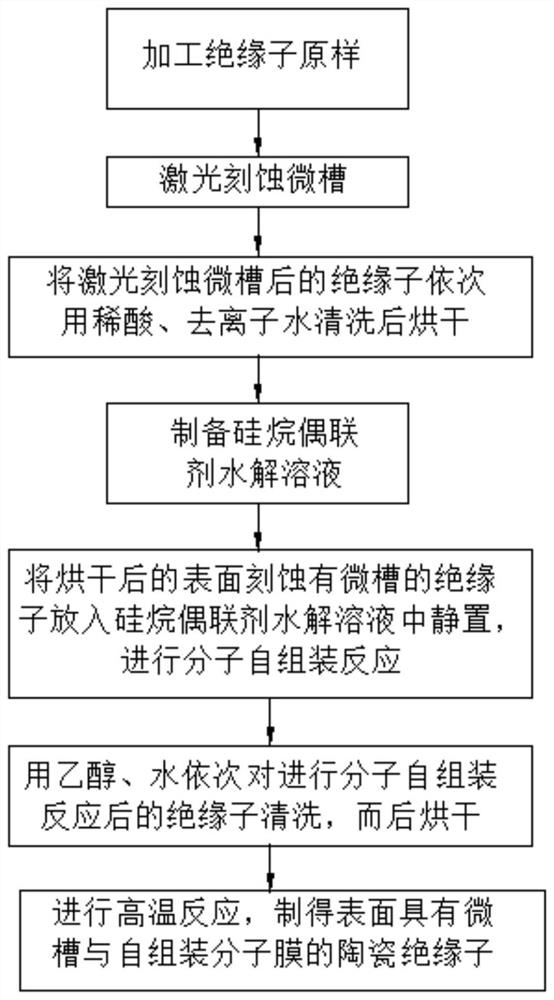
[0045] see figure 2 , the present invention also provides a method for preparing a ceramic insulator with microgrooves and self-assembled molecular films on the surface, comprising the following steps:
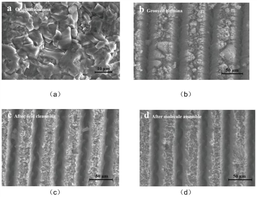
[0046] Step 1: According to the size requirements of the ceramic insulator with microgrooves and self-assembled molecular film on the surface to be prepared, process the corresponding insulator as it is; for the surface morphology of the insulator as it is, see image 3 (a);
[0047] Step 2: Turn on the laser, and set the laser parameters according to the width, depth and period size of the microgrooves that are required to be processed on the surface of the ceramic insulator with microgrooves and self-assembled molecular films on the surface to be prepared; through laser etching, the processed in step 1 Microgrooves are etched on the surface of the insulator as it is; for the surface morphology of the ceramic insulator after microgrooves are etched, see image 3 (b);
[0...
Embodiment 1
[0056] (1) Process a cylindrical alumina ceramic insulator with a diameter of 30 mm and a thickness of 10 mm as it is;
[0057] (2) Turn on the ultraviolet laser, set the laser parameters, and etch microgrooves with a width of 20 μm, a depth of 20 μm, and a period of 20 μm on the original surface of the insulator processed in step 1 by laser etching;
[0058] (3) Use a dilute hydrochloric acid solution with a concentration of 5% by mass to ultrasonically clean the insulator after the microgrooves have been etched on the surface for 30 mins to remove residual ceramic particles on the surface, clean it with deionized water, and place it in an oven at 80 ° C. Dry 12h;
[0059] (4) Weigh octadecyltrichlorosilane (OTS), toluene and deionized water according to the volume ratio of 1:20:1, then mix and stir the three evenly, prepare the toluene solution of OTS, and carry out at room temperature 0.1 hour hydrolysis to make OTS toluene hydrolysis solution;
[0060] (5) Put the insula...
Embodiment 2
[0064] (1) Process the cylindrical alumina porcelain insulator with a diameter of 30mm and a thickness of 10mm as it is;
[0065] (2) Turn on the fiber laser, set the laser parameters, and etch microgrooves with a width of 100 μm, a depth of 300 μm, and a period of 500 μm on the original surface of the insulator processed in step 1 by laser etching;
[0066] (3) Use a dilute hydrochloric acid solution with a concentration of 5% by mass to ultrasonically clean the insulator after the microgrooves have been etched on the surface for 30 mins to remove residual ceramic particles on the surface, clean it with deionized water, and place it in an oven at 80 ° C. Dry 12h;
[0067] (4) Weigh KH-550, acetone and deionized water according to the volume ratio of 1:500:1, then mix and stir the three evenly, prepare the acetone solution of KH-550, carry out hydrolysis at room temperature for 1 hour, and prepare Become the acetone hydrolysis solution of KH-550;
[0068] (5) Put the insulat...
PUM
| Property | Measurement | Unit |
|---|---|---|
| width | aaaaa | aaaaa |
| depth | aaaaa | aaaaa |
| depth | aaaaa | aaaaa |
Abstract
Description
Claims
Application Information
 - R&D
- Intellectual Property
- Life Sciences
- Materials
- Tech Scout
- Unparalleled Data Quality
- Higher Quality Content
- 60% Fewer Hallucinations
Browse by: Latest US Patents, China's latest patents, Technical Efficacy Thesaurus, Application Domain, Technology Topic, Popular Technical Reports.
© 2025 PatSnap. All rights reserved.Legal|Privacy policy|Modern Slavery Act Transparency Statement|Sitemap|About US| Contact US: help@patsnap.com


