Organic white light-emitting device and its preparation method based on stepwise multi-reaction intersystem crossing process
A light-emitting device, stepped technology, applied in semiconductor/solid-state device manufacturing, semiconductor devices, electric solid-state devices, etc., can solve the problems of low efficiency, reduced manufacturing cost, poor stability of all-fluorescent white light devices, etc., to improve luminous efficiency, The effect of reducing the preparation cost and improving the stability and lifespan
- Summary
- Abstract
- Description
- Claims
- Application Information
AI Technical Summary
Problems solved by technology
Method used
Image
Examples
Embodiment 1
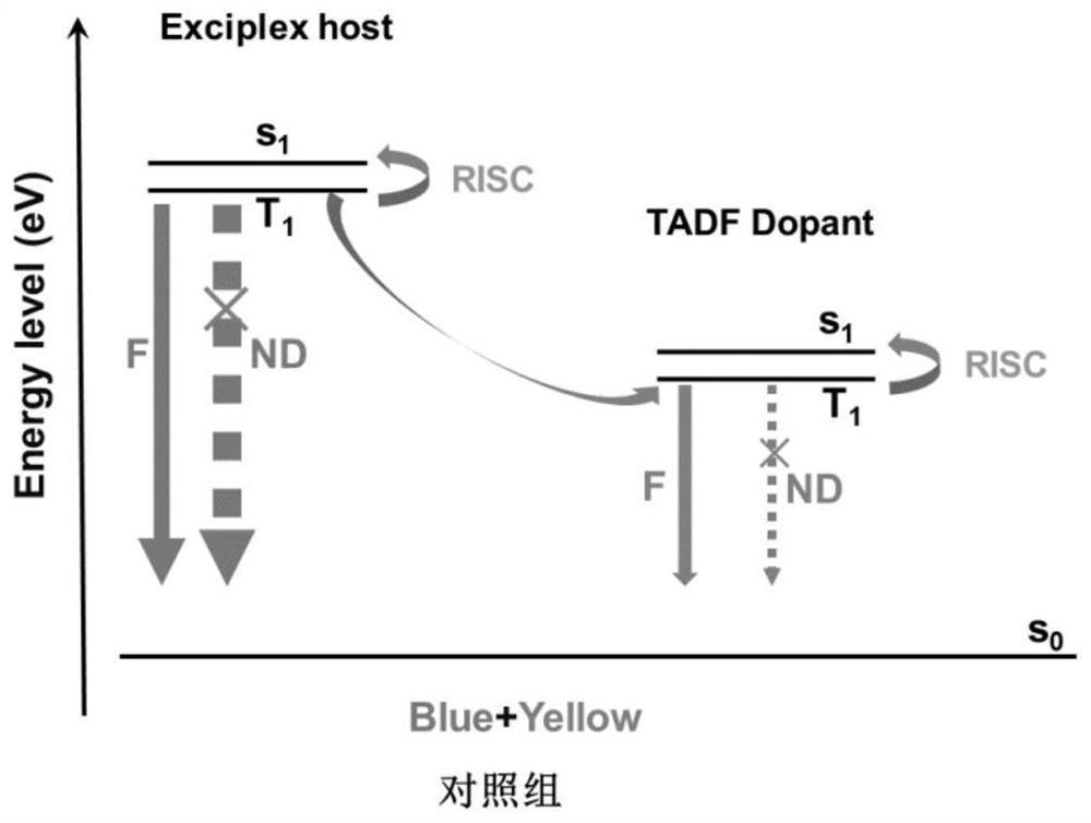
[0043] Embodiment 1: control group
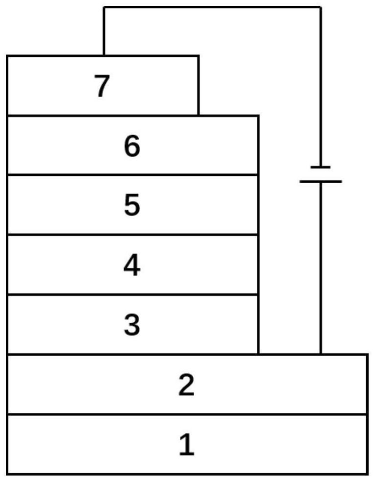
[0044] Clean the substrate composed of the substrate and the transparent conductive anode ITO, put it in a vacuum drying oven to dry after cleaning; put it in the evaporation chamber, and pump the vacuum to 3×10 -4 Pa and below, evaporate a hole transport layer with a thickness of 35nm, and evaporate a light-emitting layer on the hole transport layer (the light-emitting layer adopts ternary co-evaporation, and its ratio is controlled by the calculated rate, and the structure is traditional. The guest structure has an anti-intersystem crossing process, the materials used are MCP, 4CzPNPh, PO-T2T, the ratio of mass content is 1:0.005:1, and the thickness is 30nm), and the electron transport layer (thickness is 40nm), vapor-deposits a metal cathode (thickness is 120nm) on the electron transport layer, wherein, the evaporation rate of the organic layer is The metal cathode evaporation rate is
Embodiment 2
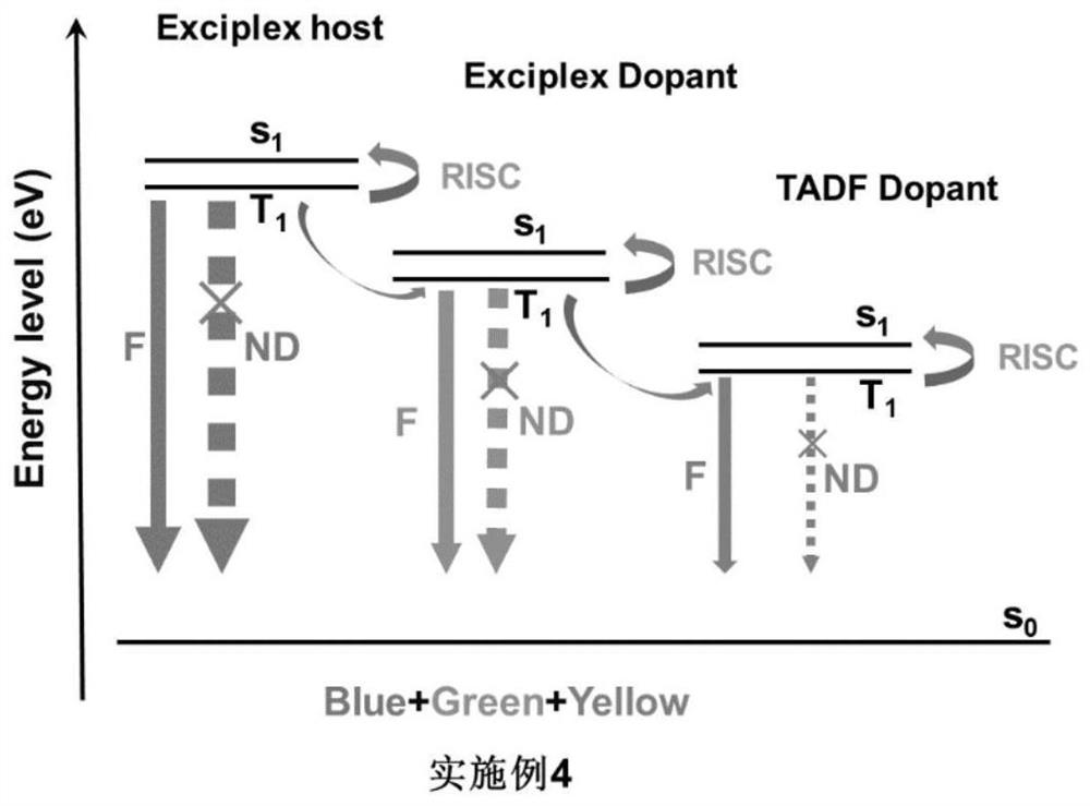
[0046]Clean the substrate composed of the substrate and the transparent conductive anode ITO, put it in a vacuum drying oven to dry after cleaning; put it in the evaporation chamber, and pump the vacuum to 3×10 -4 Pa and below, evaporate a hole transport layer with a thickness of 35nm, and evaporate a light-emitting layer on the hole transport layer (the light-emitting layer adopts ternary co-evaporation, the ratio is controlled by the calculated rate, and the structure is traditional The host-guest structure has two anti-intersystem crossing processes, the materials used are MCP, 4CzPNPh, PO-T2T, the mass content ratio is 1:0.003:1, and the thickness is 30nm), and the electron transport is evaporated on the light-emitting layer layer (thickness is 40nm), evaporate metal cathode (thickness is 120nm) on electron transport layer, wherein, organic layer evaporation rate is The metal cathode evaporation rate is
Embodiment 3
[0048] Clean the substrate composed of the substrate and the transparent conductive anode ITO, put it in a vacuum drying oven to dry after cleaning; put it in the evaporation chamber, and pump the vacuum to 3×10 -4 Pa and below, evaporate a hole transport layer with a thickness of 35nm, and evaporate a light-emitting layer on the hole transport layer (the light-emitting layer adopts ternary co-evaporation, the ratio is controlled by the calculated rate, and the structure is traditional The host-guest structure has two anti-intersystem crossing processes, the materials used are MCP, 4CzPNPh, PO-T2T, the mass content ratio is 1:0.005:1, and the thickness is 30nm), and the electron transport is evaporated on the light-emitting layer layer (thickness is 40nm), evaporate metal cathode (thickness is 120nm) on electron transport layer, wherein, organic layer evaporation rate is The metal cathode evaporation rate is
PUM
| Property | Measurement | Unit |
|---|---|---|
| thickness | aaaaa | aaaaa |
| thickness | aaaaa | aaaaa |
| thickness | aaaaa | aaaaa |
Abstract
Description
Claims
Application Information
 - R&D
- Intellectual Property
- Life Sciences
- Materials
- Tech Scout
- Unparalleled Data Quality
- Higher Quality Content
- 60% Fewer Hallucinations
Browse by: Latest US Patents, China's latest patents, Technical Efficacy Thesaurus, Application Domain, Technology Topic, Popular Technical Reports.
© 2025 PatSnap. All rights reserved.Legal|Privacy policy|Modern Slavery Act Transparency Statement|Sitemap|About US| Contact US: help@patsnap.com


