
Defect inspection device and method

A defect inspection and inspection result technology, which is applied in the field of defect inspection devices and methods, can solve the problems of position measurement circuit data output interval size error, insufficient to meet system requirements, and cannot generate timing pulses with sufficient precision, etc., to achieve image resolution The effect of improving the rate and improving the accuracy

Active Publication Date: 2020-05-12
SHANGHAI INTEGRATED CIRCUIT RES & DEV CENT +1
View PDF4 Cites 3 Cited by
  • Summary
  • Abstract
  • Description
  • Claims
  • Application Information

AI Technical Summary

Problems solved by technology

[0004] However, when the above method is used to generate the timing pulse, there will be an error in the data output interval of the position measurement circuit. Even if the fastest position measurement circuit is selected, the error may not be sufficient to meet the system requirements; The round carrier platform moves at an increased speed, and timing pulses cannot be generated with sufficient precision in the output interval of the normal laser interferometer

Method used


Image

  • Defect inspection device and method
  • Defect inspection device and method
  • Defect inspection device and method

Examples


Embodiment 1

[0075] see Figure 4 , Figure 4 Shown is a timing diagram for explaining each pulse according to the present embodiment. In this embodiment, the location information X L The update frequency is 10MHz. Therefore, location information X L The acquisition times can be at equal intervals of 100 nanoseconds. A carriage (such as the X carriage in this embodiment) can be set to move one pixel at intervals of approximately 333 nanoseconds.

[0076] Ideally, the timing pulse output time should be issued when moving one pixel. Express it as the original timing pulse output time in Figure 4 .

[0077] Because in the prior art, the output time of the comparator is used as the timing pulse, therefore, there will be an error M between the original timing pulses. The error M is equivalent to causing blur of 1 / 3 pixel. The goal in this example is to reduce this to about 1 / 10 to 1 / 100.

[0078]Therefore, in this embodiment, conventional timing pulses need to be delayed by one clock...


PUM


Abstract

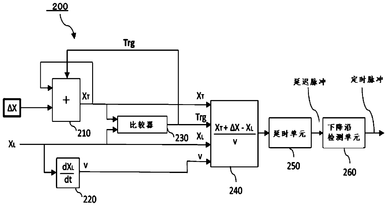
The invention provides a defect inspection device and method. The method comprises the following steps: measuring position information of an inspected object by adopting a position measurement module;according to the position information, when the inspected object moves one pixel of the camera module, generating a certain time pulse, correcting the timing pulse error, and delaying the timing pulse by one clock and then outputting the timing pulse; imaging the surface of the object to be inspected on the basis of the timing pulse delayed by one clock, and outputting an image signal; and inspecting the defects of the inspected object according to the image signal. Therefore, according to the present invention, by improving the accuracy of a timing pulse, the image resolution is improved, and an accurate trigger pulse can be generated even when slow output rate position information is used.

Description

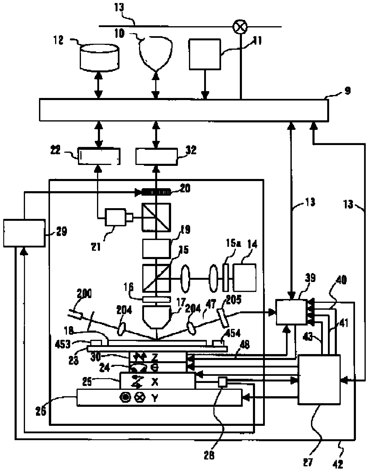
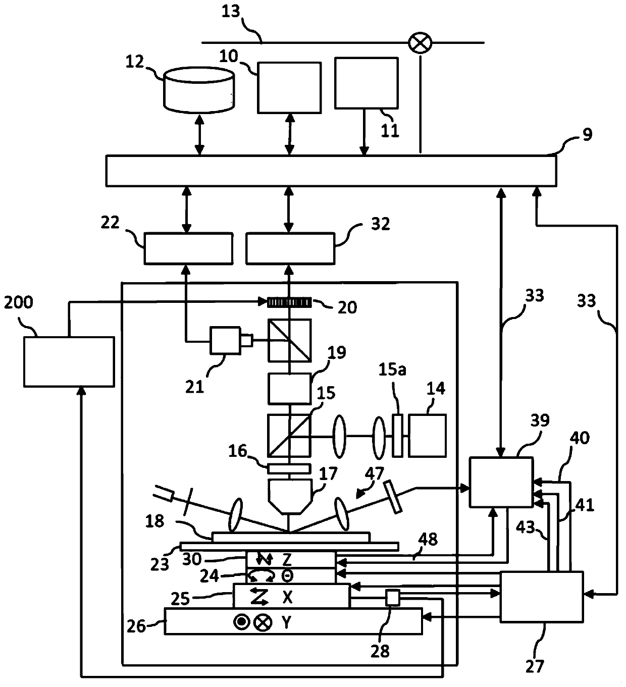
technical field [0001] The present invention relates to the field of human technology, and more particularly, relates to a defect inspection device and method. Background technique [0002] In semiconductor defect inspection systems, laser interferometers are usually used to detect the position of the carrier platform on which the wafer (inspected object) is mounted. A fixed amount of displacement of the object generates a trigger pulse (also called a "timing pulse"). [0003] see figure 1 , figure 1 Shown is a Japanese patent (Japanese Laid-Open No. 2003-177101) relating to a defect inspection device for detecting defects in wafer patterns. This device is a device for detecting the position and image of a defect on a wafer surface. as the picture shows, figure 1 There is a timing pulse generation module shown in label 29. The timing pulse generation module generates a timing pulse according to the relationship between the output data of the laser interferometer and th...

Claims


Application Information

Patent Timeline
Patent Type & Authority Applications(China)
IPC IPC(8): H01L21/66H01L21/67
CPCH01L22/24H01L22/20H01L21/67253
Inventor 玉虫秀一李琛赵宇航李铭卢意飞王鹏飞
Owner SHANGHAI INTEGRATED CIRCUIT RES & DEV CENT
Learn More