Stereo Electromagnetic Bandgap Circuit

An electromagnetic energy, three-dimensional technology, applied in circuit devices, printed circuit components, reduction of crosstalk/noise/electromagnetic interference (etc.) Effect, the effect of improving elasticity

Active Publication Date: 2021-04-23
REALTEK SEMICON CORP
View PDF5 Cites 0 Cited by
  • Summary
  • Abstract
  • Description
  • Claims
  • Application Information

AI Technical Summary

Problems solved by technology

[0002] The electromagnetic energy gap structure can be used to suppress the propagation of electromagnetic wave noise, but the traditional electromagnetic energy gap structure is mostly a planar structure, which requires a large circuit area
[0003] When the circuit space inside the electronic device is not enough, it is difficult to set a sufficient number of electromagnetic energy gap structural units, which will reduce the ability to suppress the propagation of electromagnetic wave noise

Method used


Image

  • Stereo Electromagnetic Bandgap Circuit
  • Stereo Electromagnetic Bandgap Circuit
  • Stereo Electromagnetic Bandgap Circuit

Examples


Embodiment Construction

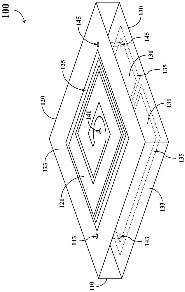
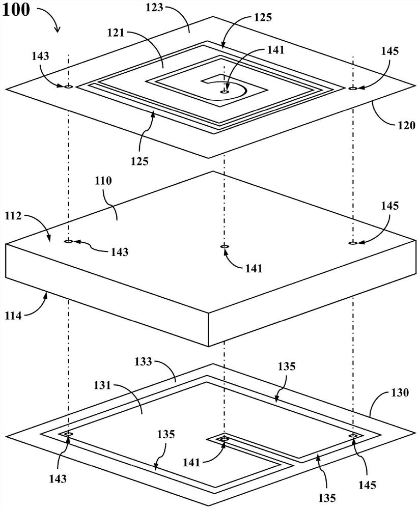
[0044] Embodiments of the present invention will be described below in conjunction with related drawings. In the drawings, the same reference numerals designate the same or similar elements.

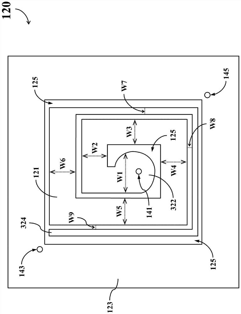
[0045] Please refer to Figure 1 to Figure 4 . figure 1 It is a simplified structural diagram of the three-dimensional electromagnetic bandgap circuit 100 according to an embodiment of the present invention. figure 2 It is a schematic structural diagram of the three-dimensional electromagnetic bandgap circuit 100 after decomposition. image 3 It is a simplified schematic diagram of the first embodiment of the first layer structure 120 of the three-dimensional electromagnetic bandgap circuit. Figure 4 It is a simplified schematic diagram of the first embodiment of the second layer structure 130 of the three-dimensional electromagnetic bandgap circuit.

[0046] The three-dimensional electromagnetic bandgap circuit 100 can be arranged in a circuit board with a double-layer board struc...


PUM


Abstract

The present invention proposes a three-dimensional electromagnetic bandgap circuit, comprising: a dielectric layer having a first surface and an opposite second surface; a helical element located on the first surface; a first surrounding element located on the first surface, and wraps around the helical element but does not touch the helical element; the planar element is on the second surface and includes a notch; the second wrapping element is on the second surface and wraps around the planar element but does not contact the planar element, wherein the second surrounding element also includes a protrusion extending toward the gap; the first guide hole penetrates the dielectric layer, the spiral element, and the protrusion; the second guide hole penetrates the dielectric layer, The planar element, and the first surrounding element; and the third guide hole, passing through the dielectric layer, the planar element, and the first surrounding element.

Description

technical field [0001] The present invention relates to an electromagnetic bandgap structure, in particular to a three-dimensional electromagnetic bandgap circuit (3D electromagnetic bandgap circuit, three-dimensional electromagnetic bandgap circuit). Background technique [0002] The electromagnetic bandgap structure can be used to suppress the propagation of electromagnetic wave noise, but the traditional electromagnetic bandgap structure is mostly a planar structure, which requires a large circuit area. [0003] When the circuit space inside the electronic device is insufficient, it is difficult to arrange a sufficient number of electromagnetic energy gap structural units, which will reduce the ability to suppress the propagation of electromagnetic wave noise. Contents of the invention [0004] In view of this, how to effectively reduce the circuit area occupied by the electromagnetic bandgap structure is a problem to be solved. [0005] This specification provides an ...

Claims


Application Information

Patent Timeline
Patent Type & Authority Patents(China)
IPC IPC(8): H05K1/02
CPCH05K1/0236
Inventor 汪余聪吴瑞北王世宏王文山
Owner REALTEK SEMICON CORP
Why Eureka
Try Eureka