Mini LED packaging method and Mini LED

A packaging method and LED chip technology, which is applied in the direction of electrical components, electric solid devices, circuits, etc., can solve problems such as random arrangement and shape, and achieve the effect of random arrangement, precise arrangement size and good density

Active Publication Date: 2019-11-08
厦门多彩光电子科技有限公司
View PDF8 Cites 2 Cited by
  • Summary
  • Abstract
  • Description
  • Claims
  • Application Information

AI Technical Summary

Problems solved by technology

However, it also has the following disadvantages. Each lamp bead is independently electrically connected to the substrate, which requires the corresponding connection electrodes to be provided on the substrate first. The structure of the lamp beads is limited to the layout of the connection electrodes on the substrate. Therefore, Unable to arbitrarily arrange shapes

Method used


Image

  • Mini LED packaging method and Mini LED
  • Mini LED packaging method and Mini LED
  • Mini LED packaging method and Mini LED

Examples


Embodiment 1

[0029] refer to figure 1 As shown, the present invention provides a packaging method for Mini LEDs, comprising the following steps:

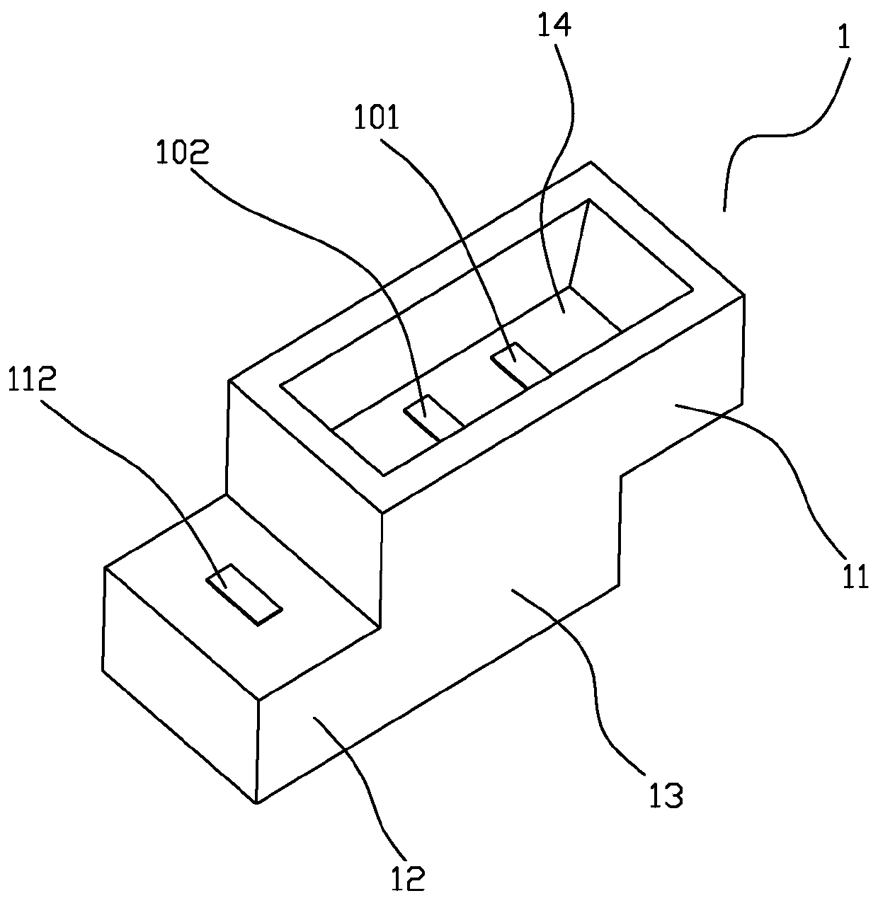
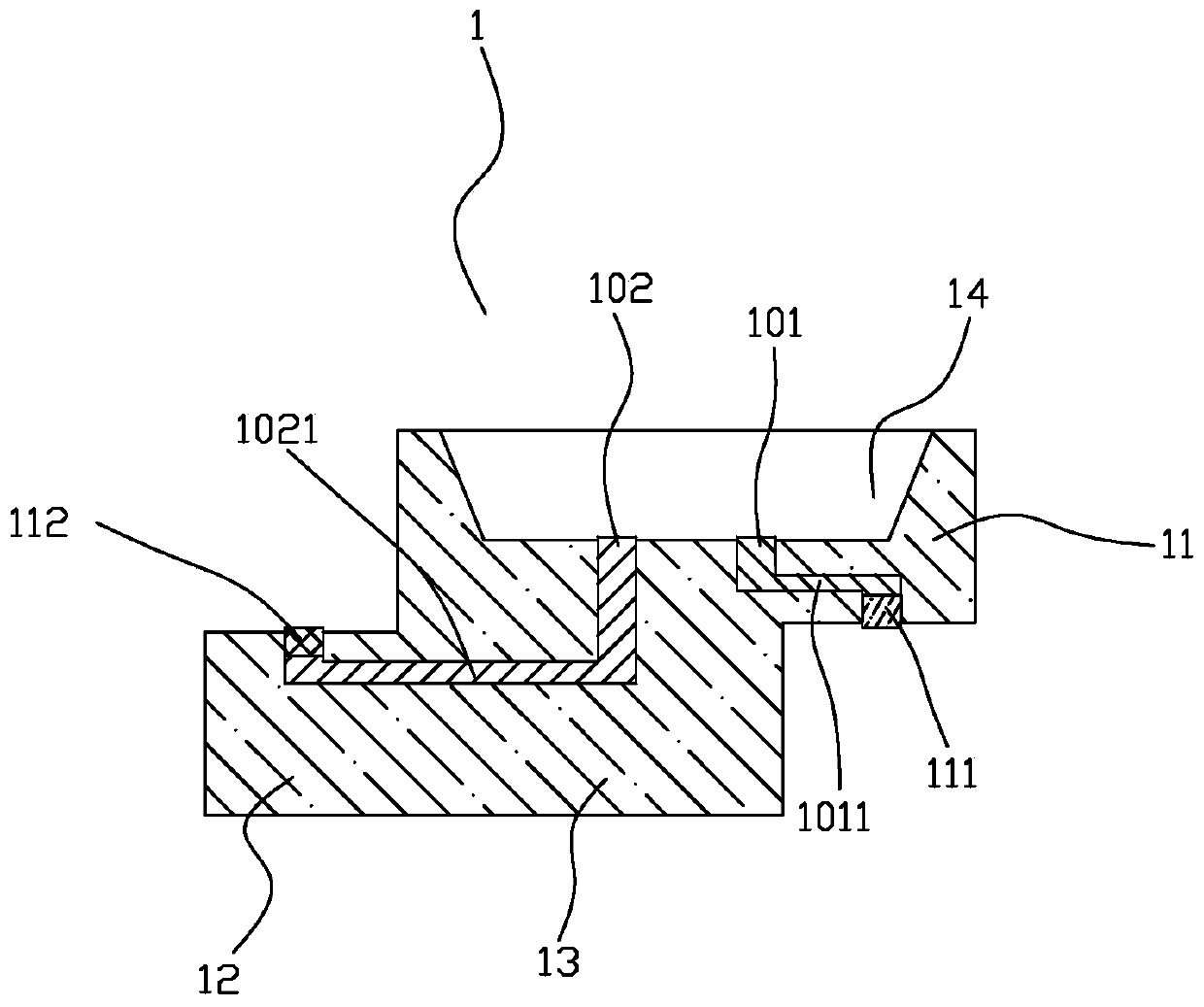
[0030] A1, provides package holder 1, such as figure 2 , image 3 As shown, the package holder has a "Z" shape structure, including a package part 13, a first pin part 11 connected to an upper position on one side of the package part 13, and a first pin part 11 connected to a lower position on the other side of the package part 13. Two lead parts 12, the upper surface of the package part 13 is flush with the upper surface of the first lead part 11 and forms a package surface, the package surface is provided with a first electrode 101 and a second electrode with opposite polarities 102 (i.e. positive electrode and negative electrode), the lower surface of the first pin part 11 is provided with a first contact 111 connected to the first electrode 101, and the upper surface of the second pin part 12 is provided with a first contact 111 connected...


PUM


Abstract

The invention provides a Mini LED packaging method and a Mini LED prepared through the method. A package support is set in a "Z"-shape structure; after package molding, photoelectric detection is performed; then, array arrangement is carried out to form a required patterned Mini LED light-emitting module, and yield is good; the "Z"-shaped structure is easy to assemble, that is, a second pin portion and a first pin portion of adjacent lamp bead units are overlapped and cooperated and are in electrical connection; the connection structure is compact, density is good, arrangement size is accurateand no deviation is caused; and chip package can be carried out without arranging an electrode on a substrate, so that the limitation of the substrate electrode is eliminated, and free arrangement isachieved.

Description

technical field [0001] The invention relates to the field of semiconductor lighting and display, in particular to a packaging method of Mini LED and the Mini LED prepared by the method. Background technique [0002] Mini LED refers to a display screen that uses more precise devices and new packaging methods to achieve 0.2-0.9 mm pixel particles. With the decline of LED chip costs and technological progress, coupled with the recent sluggish growth of the LED lighting industry, LED chip and packaging giants at home and abroad have begun to look for new market growth points. At present, Micro LED is difficult to be commercialized on a large scale in a short period of time due to the uncertain technical route and high cost. Mini LED, as an extension of small-pitch LED products and a prelude to Micro LED, has begun to be used in LCD Backlight and RGB display products were shipped. [0003] Traditional Mini LEDs generally use cob (chip On board) packaging, which is to directly p...

Claims


Application Information

Patent Timeline
Patent Type & Authority Applications(China)
IPC IPC(8): H01L25/075H01L33/00H01L33/54H01L33/62
CPCH01L25/0753H01L33/005H01L33/54H01L33/62
Inventor 温小斌苏水源郑剑飞
Owner 厦门多彩光电子科技有限公司
Why Eureka
Try Eureka