Full-automatic silicon wafer cleaning device

A silicon wafer cleaning, fully automatic technology, applied in cleaning methods and utensils, cleaning methods using tools, cleaning methods using liquids, etc., can solve problems such as difficult cleaning machine removal, manual placement of wafer baskets, device failure, etc.

Pending Publication Date: 2019-10-15
ZHEJIANG UNIVERSITY OF SCIENCE AND TECHNOLOGY
View PDF0 Cites 6 Cited by
  • Summary
  • Abstract
  • Description
  • Claims
  • Application Information

AI Technical Summary

Problems solved by technology

Trace contamination can also lead to device failure
The purpose of cleaning is to remove oily impurities on the surface, including organic and inorganic substances. Some of these impurities exist on the surface of the silicon wafer in the form of atoms or ions, and some exist in the form of thin films or particles. Due to the electrostatic effect, it is difficult to be cleaned by the cleaning machine, and the current cleaning machine is not highly automated, and it is necessary to manually place the basket and load the material

Method used


Image

  • Full-automatic silicon wafer cleaning device
  • Full-automatic silicon wafer cleaning device
  • Full-automatic silicon wafer cleaning device

Examples


Embodiment Construction

[0018] The technical solutions of the present invention will be clearly and completely described below in conjunction with the accompanying drawings. Apparently, the described embodiments are some of the embodiments of the present invention, but not all of them. Based on the embodiments of the present invention, all other embodiments obtained by persons of ordinary skill in the art without making creative efforts belong to the protection scope of the present invention.

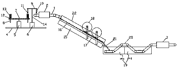
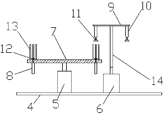
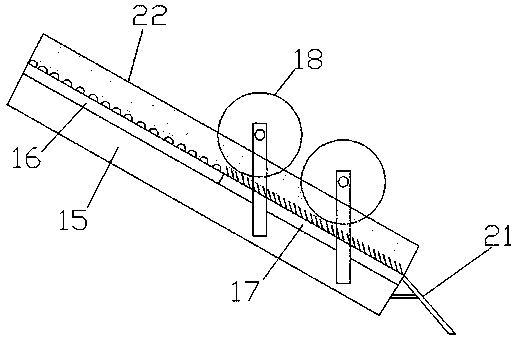
[0019] Such as Figure 1~4 As shown, the present invention provides a fully automatic silicon wafer cleaning device, including a feeding mechanism, a conveyor belt 1, a static elimination channel 2, an auxiliary unloading mechanism, an ultrasonic cleaning mechanism, and a drying channel 3. The feeding mechanism includes a bottom plate 4 , stepper motor 5, corner motor 6, turntable 7, electric telescopic rod 8, horizontal suspension rod 9, telescopic cylinder 10, vacuum sucker 11, described stepper motor 5, cor...


PUM


Abstract

The invention discloses a full-automatic silicon wafer cleaning device. The full-automatic silicon wafer cleaning device comprises a feeding mechanism, a conveying belt, an electrostatic removal channel, an auxiliary discharging mechanism, an ultrasonic cleaning mechanism and a drying channel. The full-automatic silicon wafer cleaning device is novel in structure, low in manufacturing cost and high in automation degree; and a silicon wafer sequentially passes through the feeding mechanism, the conveying belt, the electrostatic removal channel, the auxiliary discharging mechanism, the ultrasonic cleaning mechanism and the drying channel, and thus automatic feeding, automatic cleaning, automatic drying and discharging of silicon wafers are achieved, the operation is simple and convenient, the production time is greatly shortened, and the working efficiency is improved.

Description

technical field [0001] The invention relates to the field of semiconductor silicon wafer processing, in particular to a fully automatic silicon wafer cleaning device. Background technique [0002] Silicon wafers must be strictly cleaned in the production of semiconductor devices. Trace contamination can also lead to device failure. The purpose of cleaning is to remove oily impurities on the surface, including organic and inorganic substances. Some of these impurities exist on the surface of the silicon wafer in the form of atoms or ions, and some exist in the form of thin films or particles. Due to the electrostatic effect, it is difficult to be cleaned by the washing machine, and the current washing machine is not highly automated, and it is necessary to manually place the basket and load the material. Contents of the invention [0003] The object of the present invention is to provide a fully automatic silicon wafer cleaning device to solve the problems raised in the a...

Claims


Application Information

Patent Timeline
IPC IPC(8): B08B1/00B08B1/02B08B3/12H01L21/67
CPCB08B3/123H01L21/67028H01L21/6704H01L21/67034B08B1/20B08B1/12
Inventor 侯继伟
Owner ZHEJIANG UNIVERSITY OF SCIENCE AND TECHNOLOGY
Why Eureka
Try Eureka