
Display panel and method of fabricating the same

A display panel and manufacturing method technology, applied in nonlinear optics, instruments, optics, etc., can solve the problems of large contact impedance in the binding area of ​​the display panel, wide frame of the display panel, etc., so as to avoid severe electrical signal degradation and reduce the frame , improve the display effect and the effect of

Active Publication Date: 2019-08-09
SHENZHEN CHINA STAR OPTOELECTRONICS SEMICON DISPLAY TECH CO LTD
View PDF16 Cites 37 Cited by
  • Summary
  • Abstract
  • Description
  • Claims
  • Application Information

AI Technical Summary

Problems solved by technology

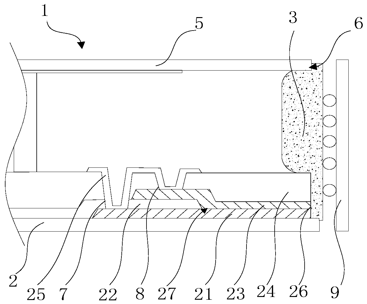
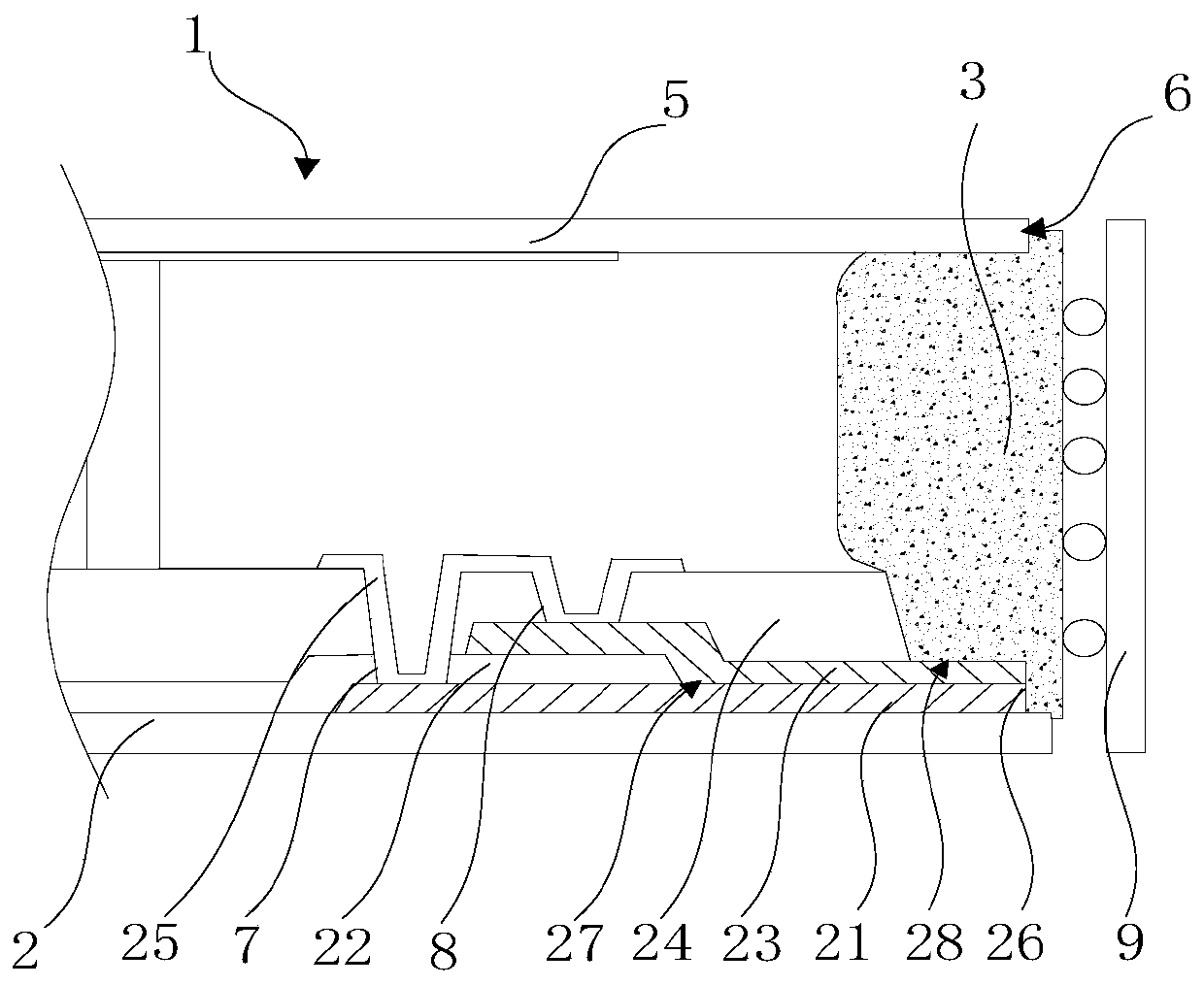
[0004] The embodiment of the present application provides a display panel and a manufacturing method of the display panel to solve the technical problems of wide frame of the display panel and large contact impedance of the binding area of ​​the display panel

Method used


Image

  • Display panel and method of fabricating the same
  • Display panel and method of fabricating the same
  • Display panel and method of fabricating the same

Examples


Embodiment Construction

[0039] Specific structural and functional details disclosed herein are representative only and for purposes of describing example embodiments of the present invention. This invention may, however, be embodied in many alternative forms and should not be construed as limited to only the embodiments set forth herein.

[0040] In describing the present invention, it is to be understood that the terms "central", "lateral", "upper", "lower", "left", "right", "vertical", "horizontal", "top", The orientation or positional relationship indicated by "bottom", "inner", "outer", etc. is based on the orientation or positional relationship shown in the drawings, and is only for the convenience of describing the present invention and simplifying the description, rather than indicating or implying the referred device Or elements must have a certain orientation, be constructed and operate in a certain orientation, and thus should not be construed as limiting the invention. In addition, the te...


PUM


Abstract

he application discloses a display panel and a method of fabricating the same. The display panel comprises a first metal layer, an insulating layer, a second metal layer, and a bonding electrode. Theinsulating layer is disposed on the first metal layer and has a first excavation part for exposing the first metal layer. The second metal layer is arranged on the insulating layer and extends to thebottom of the first excavation part to cover the exposed first metal layer. The bonding electrode is formed on the same sides of the first metal layer and the second metal layer. According to the application, the contact area between the first metal layer and the second metal layer that are electrically connected to the bonding electrode is increased; the contact resistance between the first metallayer and the second metal layer is reduced; the burning of the bonding area of the abnormal picture area and the display panel is avoided; and the display effect and the yield of the display panel are improved.

Description

technical field [0001] The present application relates to the technical field of display panels, in particular to a display panel and a method for manufacturing the display panel. Background technique [0002] With the improvement of the liquid crystal display (Liquid Crystal Display, LCD) performance and the COF (Chip On Flex, or, Chip On Film, often called chip on film) binding process, splicing screen technology has been widely used in panel production. The screen market has a wide range of applications, and can be applied to commercial display, outdoor, security monitoring, etc. Most of the existing splicing screens are spliced ​​with multiple sub-display panels, and two adjacent sub-display panels always have areas that cannot be displayed in the splicing area, which is the so-called splicing gap, or splicing seam for short. The seam on the splicing screen affects the display effect. Therefore, narrowing the seam technology has many advantages, such as Ultra Narrow bor...

Claims


Application Information

Patent Timeline
Patent Type & Authority Applications(China)
IPC IPC(8): G02F1/1345G02F1/1333
CPCG02F1/133345G02F1/1345G02F1/13452
Inventor 陈仁禄叶岩溪
Owner SHENZHEN CHINA STAR OPTOELECTRONICS SEMICON DISPLAY TECH CO LTD
Learn More