Liquid crystal display panel, manufacturing method thereof, and display device

A technology of liquid crystal display panel and manufacturing method, which is applied in the direction of instruments, nonlinear optics, optics, etc., which can solve the problems of missing electrodes, decreased transmittance, and decreased aperture ratio of pixel units, so as to achieve brightness and contrast and increase light leakage area Effect

Active Publication Date: 2021-11-16
KUSN INFOVISION OPTOELECTRONICS
View PDF0 Cites 0 Cited by
  • Summary
  • Abstract
  • Description
  • Claims
  • Application Information

AI Technical Summary

Problems solved by technology

In the state of wide viewing angle, the sub-pixel electrode corresponding to the W sub-pixel is missing and does not participate in the display screen, resulting in a decrease in the aperture ratio of the pixel unit in the wide viewing angle state, resulting in a decrease in transmittance

Method used


Image

  • Liquid crystal display panel, manufacturing method thereof, and display device
  • Liquid crystal display panel, manufacturing method thereof, and display device
  • Liquid crystal display panel, manufacturing method thereof, and display device

Examples


Embodiment Construction

[0035] In order to further explain the technical means and effects of the present invention to achieve the intended purpose of the invention, the specific implementation, structure, features and effects of the present invention will be described in detail below in conjunction with the accompanying drawings and examples.

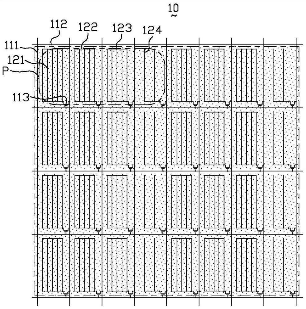
[0036] like figure 1 and figure 2 As shown, the liquid crystal display panel 100 provided in this embodiment includes an array substrate 10 , a color filter substrate 30 and a liquid crystal layer 20 sandwiched between the array substrate 10 and the color filter substrate 30 . The liquid crystal display panel 100 is provided with a plurality of pixel units P, and each pixel unit P includes a first area PA and a second area PB, and the first area PA is provided with a red sub-pixel electrode 121, a green sub-pixel electrode 122, a blue A sub-pixel electrode 123, the second area PB is provided with a white sub-pixel electrode 124, and each pixel unit P is als...


PUM


Abstract

The present invention provides a liquid crystal display panel, a manufacturing method thereof, and a display device. The liquid crystal display panel is provided with a plurality of pixel units, each pixel unit includes a first area and a second area, and the first area is provided with a red sub-pixel electrode, The green sub-pixel electrode and the blue sub-pixel electrode, the second area is provided with a white sub-pixel electrode, and each pixel unit is also provided with a first common electrode and a second common electrode, and each sub-pixel electrode in the first area is connected to the first common electrode. The electrodes are located in different layers and arranged up and down, the white sub-pixel electrodes in the second area and the second common electrode are on the same plane, and the viewing angle control electrodes are arranged on the color filter substrate corresponding to the positions of the white sub-pixel electrodes. By dividing the pixel unit into the first area and the second area, when the wide viewing angle is displayed, each sub-pixel participates in the picture display, and when the narrow viewing angle is displayed, the white sub-pixel electrode in the second area does not participate in the picture display, realizing the brightness and brightness of the wide and narrow viewing angles. The contrast ratio is consistent, and the penetration rate of the wide viewing angle display can be improved at the same time.

Description

technical field [0001] The invention relates to the field of display technology, and in particular to a liquid crystal display panel with switching between wide and narrow viewing angles, a manufacturing method thereof, and a display device. Background technique [0002] Liquid crystal display (liquid crystal display, LCD) has the advantages of good image quality, small size, light weight, low driving voltage, low power consumption, no radiation and relatively low manufacturing cost, and occupies a dominant position in the field of flat panel display. [0003] Currently, liquid crystal display devices are gradually developing toward wide viewing angles. For example, liquid crystal display devices using in-plane switching (IPS) or fringe field switching (FFS) modes can achieve wider viewing angles. The wide viewing angle design allows users to see a complete and undistorted picture from all directions. However, in today's society, people pay more and more attention to protec...

Claims


Application Information

Patent Timeline
Patent Type & Authority Patents(China)
IPC IPC(8): G02F1/1343G02F1/13
CPCG02F1/1323G02F1/134309
Inventor 钟德镇乔艳冰柯中乔刘建玮
Owner KUSN INFOVISION OPTOELECTRONICS
Why Eureka
Try Eureka