A circuit board defect detection method and device

A defect detection and circuit board technology, applied in image data processing, instruments, biological neural network models, etc., can solve the problems of high detection cost, low accuracy, low efficiency, etc., and achieve the effect of improving accuracy and efficiency

Inactive Publication Date: 2019-06-14
BEIJING BAIDU NETCOM SCI & TECH CO LTD
View PDF5 Cites 13 Cited by
  • Summary
  • Abstract
  • Description
  • Claims
  • Application Information

AI Technical Summary

Problems solved by technology

[0005] This application proposes a circuit board defect detection method and device, which solves the technical problems of low accuracy, high detection cost and low efficiency in the prior art when the circuit board defect detection relies on manual detection

Method used


Image

  • A circuit board defect detection method and device
  • A circuit board defect detection method and device
  • A circuit board defect detection method and device

Examples


Embodiment Construction

[0052] Embodiments of the present application are described in detail below, examples of which are shown in the drawings, wherein the same or similar reference numerals denote the same or similar elements or elements having the same or similar functions throughout. The embodiments described below by referring to the figures are exemplary, and are intended to explain the present application, and should not be construed as limiting the present application.

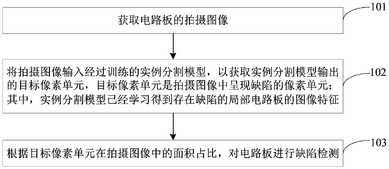
[0053] The embodiment of this application aims at the technical problems of high detection cost, low accuracy of detection results and poor real-time performance in the prior art where the detection of circuit board defects relies on purely manual detection methods, and proposes a circuit board defect detection method.

[0054] The circuit board defect detection method provided by the embodiment of the present application obtains the captured image of the circuit board, and inputs the captured image into the trained instance s...


PUM


Abstract

The invention provides a circuit board defect detection method and device, wherein the method comprises the steps of obtaining a shooting image of a circuit board, inputting the shooting image into atrained instance segmentation model, obtaining a target pixel unit output by the instance segmentation model, and enabling the target pixel unit to be a pixel unit presenting defects in the shooting image, wherein the instance segmentation model learns to obtain image characteristics of the local circuit board with the defect, and defect detection is carried out on the circuit board according to the area proportion of the target pixel unit in the shot image. As the instance segmentation model learns to obtain the image features of the local circuit board with the defects, the target pixel unitwith the defect can be accurately positioned in the shot image, further verification is carried out according to the area proportion of the target pixel unit in the shot image so as to finally determine whether the circuit board has the defect, and the defect detection precision and efficiency of the detected circuit board can be improved.

Description

technical field [0001] The present application relates to the technical field of deep learning and image processing, and in particular to a method and device for detecting defects of circuit boards. Background technique [0002] At present, circuit board manufacturing relies on automated industrial production lines. Due to the increasing integration of electronic components of circuit boards, the production process of circuit boards is becoming more and more complicated. Defective circuit boards will inevitably appear during the process of circuit board generation. Therefore, Defect detection on the circuit board can avoid circuit board damage caused by defects. [0003] In the prior art, circuit board production enterprises mainly use manual detection methods to detect defects on circuit boards. However, manual inspection requires staff to inspect with naked eyes, which has the disadvantages of high detection cost, low accuracy, and low efficiency. Contents of the invent...

Claims


Application Information

Patent Timeline
IPC IPC(8): G06T7/00G06T7/11G06T7/62G06N3/04
Inventor 文亚伟苏业刘明浩郭江亮李旭
Owner BEIJING BAIDU NETCOM SCI & TECH CO LTD
Why Eureka
Try Eureka