
Bottom emission white light organic light emitting diode display panel, manufacturing method thereof, and display device

A technology for light-emitting diodes and display panels, which is applied in the manufacture of semiconductor/solid-state devices, semiconductor devices, electrical components, etc., can solve the problems of high power consumption, low color purity, and low energy utilization rate of panels, and achieves lower power consumption, higher Color gamut performance, the effect of increasing energy utilization efficiency

Active Publication Date: 2020-11-10
SHENZHEN CHINA STAR OPTOELECTRONICS SEMICON DISPLAY TECH CO LTD
View PDF4 Cites 0 Cited by
  • Summary
  • Abstract
  • Description
  • Claims
  • Application Information

AI Technical Summary

Problems solved by technology

Due to the wide spectrum of white light, when using a color filter (CF) to separate white light into RGB three primary colors, the RG spectrum is usually wide and the color purity is low, and the color gamut performance of the panel is difficult to break through the 100 set by NTSC %standard
In addition, when white light is separated into RG spectrum, only a small amount of red or green light in the white light spectrum can be used, and the energy loss of blue and yellow light is relatively large.
Therefore, due to the low energy utilization rate of the existing WOLED, it will cause the problem of high power consumption when the panel is working.

Method used


Image

  • Bottom emission white light organic light emitting diode display panel, manufacturing method thereof, and display device
  • Bottom emission white light organic light emitting diode display panel, manufacturing method thereof, and display device
  • Bottom emission white light organic light emitting diode display panel, manufacturing method thereof, and display device

Examples


Embodiment Construction

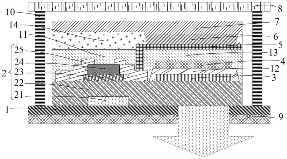
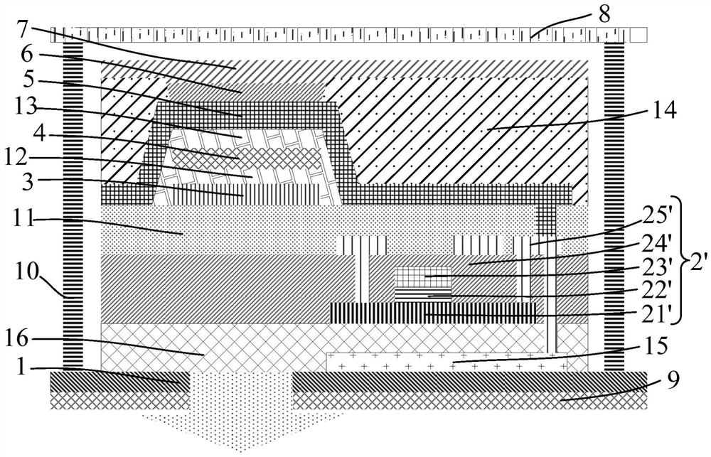
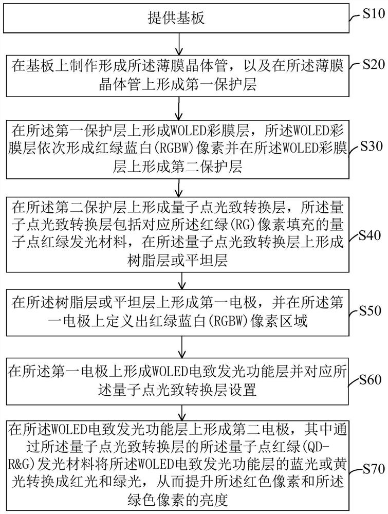
[0031]Reference in the detailed description to "an embodiment" means that a particular feature, structure, or characteristic described in connection with the embodiment can be included in at least one embodiment of the invention. The same terms appearing in different positions in the specification are not necessarily limited to the same implementation, but should be understood as independent or alternative implementations from other embodiments. Inspired by the technical solutions disclosed in the embodiments provided in the present invention, those skilled in the art should understand that the embodiments described in the present invention may have other combinations or changes of technical solutions consistent with the concept of the present invention.

[0032] The following descriptions of the various embodiments refer to the accompanying drawings to illustrate specific embodiments in which the present invention can be practiced. The directional terms mentioned in the prese...


PUM

PropertyMeasurementUnit
thicknessaaaaaaaaaa
thicknessaaaaaaaaaa

Abstract

A bottom emission white light organic light emitting diode display panel and its manufacturing method, display device, wherein the bottom emission WOLED display panel includes a substrate, a thin film transistor, a WOLED color filter layer, a quantum dot photoelectric conversion layer, a first electrode, a WOLED electric A luminescent functional layer and a second electrode. The WOLED color filter layer is provided with red, green, blue and white pixels in sequence. The quantum dot phototransformation layer includes quantum dot red and green luminescent materials corresponding to the red and green pixels. The WOLED electroluminescent functional layer is arranged on the first electrode. The second electrode is arranged on the WOLED electroluminescent functional layer, and the blue light or yellow light of the WOLED electroluminescent functional layer is converted into red by the quantum dot red-green luminescent material of the quantum dot phototransformation layer. light and green light, so as to increase the brightness of the red pixel and the green pixel, so as to improve the color gamut performance of the bottom emission WOLED display panel.

Description

technical field [0001] The invention relates to the field of display technology, in particular to a bottom emission white light organic light emitting diode (WOLED) display panel, a manufacturing method thereof, and a display device. Background technique [0002] Organic light-emitting diode (OLED) is a new type of display technology. Compared with LCD display technology, it has active light emission, true color, infinite contrast, zero delay, transparent display, flexible display, free-form display (Free-Form D insulation It is a next-generation display technology that can replace liquid crystal display technology. Since OLED display technology does not require a backlight source, its structure is simpler than that of LCD, and the volume of display products can be made lighter and thinner. White organic light-emitting diodes (WOLED) are mainly used in large-size panel display technology. WOLED technology is different from the side-by-side (side-by-side) RGB technology wide...

Claims


Application Information

Patent Timeline
Patent Type & Authority Patents(China)
IPC IPC(8): H01L51/50H01L51/52H01L51/56H01L27/32
CPCH10K59/8722H10K59/871
Inventor 吴元均袁伟矫士博
Owner SHENZHEN CHINA STAR OPTOELECTRONICS SEMICON DISPLAY TECH CO LTD
Learn More