Circuit topology structure of large-power charging/discharging system and control method of structure
A circuit topology, charge and discharge technology, applied in the direction of output power conversion device, reactive power adjustment/elimination/compensation, AC power input conversion to DC power output, etc.
- Summary
- Abstract
- Description
- Claims
- Application Information
AI Technical Summary
Problems solved by technology
Method used
Image
Examples
specific Embodiment approach 1
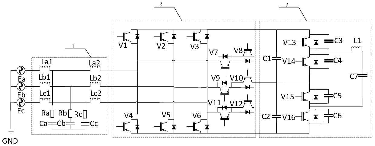
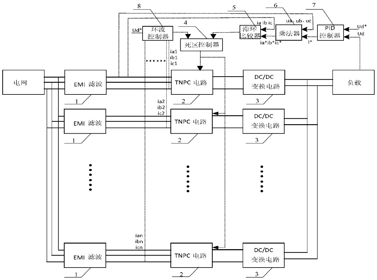
[0027] Specific implementation mode one: the following combination figure 1 Describe this embodiment, a high-power charging and discharging system circuit topology described in this embodiment, which includes n EMI filter circuits 1, n TNPC circuits 2, n DC / DC conversion circuits 3, and a dead zone controller 4 , hysteresis comparator 5, multiplier 6, PID controller 7 and circulation controller 8;
[0028] An EMI filter circuit 1 is connected in series with a TNPC circuit 2 and a DC / DC conversion circuit 3 to form a set of converter circuits, and n sets of converter circuits are connected in parallel and then connected in series between the power grid and the load;
[0029] The voltage signal input terminal of the circulating current controller 8 inputs the preset DC voltage Ud * ; 0-t time, the circulation controller 8 simultaneously inputs the feed-forward control signal to the control signal input end of the TNPC circuit 2 of each group of converter circuits;
[0030] Aft...
specific Embodiment approach 2
[0036] Specific implementation mode two: the following combination figure 2Describe this embodiment. This embodiment further describes the circuit topology of a high-power charging and discharging system described in Embodiment 1. It also includes a dead zone controller 4, and the signal input terminal of the dead zone controller 4 is connected to the circulating current The feedforward signal output terminal of the controller 8 and the signal output terminal of the hysteresis comparator 5 .
specific Embodiment approach 3
[0037] Specific implementation mode three: the following combination figure 2 Describe this embodiment, this embodiment will further explain the circuit topology of a high-power charging and discharging system described in Embodiment 1 or 2, EMI filter circuit 1 includes a resistor Ra, a resistor Rb, a resistor Rc, a capacitor Ca, and a capacitor Cb , capacitance Cc, inductance La1, inductance La2, inductance Lb1, inductance Lb2, inductance Lc1 and inductance Lc2;
[0038] One end of the inductor La1 is connected to the output terminal of the a-phase power supply of the AC power supply, the other end of the inductor La1 is connected to one end of the resistor Ra and one end of the inductor La2 at the same time, and the other end of the resistor Ra is connected to one end of the capacitor Ca;
[0039] One end of the inductor Lb1 is connected to the b-phase power output terminal of the AC power supply, the other end of the inductor Lb1 is connected to one end of the resistor Rb...
PUM
 Abstract
Description
Claims
Application Information
 - Generate Ideas
- Intellectual Property
- Life Sciences
- Materials
- Tech Scout
- Unparalleled Data Quality
- Higher Quality Content
- 60% Fewer Hallucinations
Browse by: Latest US Patents, China's latest patents, Technical Efficacy Thesaurus, Application Domain, Technology Topic, Popular Technical Reports.
© 2025 PatSnap. All rights reserved.Legal|Privacy policy|Modern Slavery Act Transparency Statement|Sitemap|About US| Contact US: help@patsnap.com


