Display substrate and manufacturing method thereof, and display panel

A technology for display substrates and isolation layers, which is applied in semiconductor/solid-state device manufacturing, organic semiconductor devices, semiconductor devices, etc., and can solve problems affecting display performance, etc.

Active Publication Date: 2019-05-10
BOE TECH GRP CO LTD +1
View PDF10 Cites 6 Cited by
  • Summary
  • Abstract
  • Description
  • Claims
  • Application Information

AI Technical Summary

Problems solved by technology

[0004] The purpose of the present invention is to at least partially solve the problem that the display performance of the display substrate will be affected when the brightness unevenness is improved, and to provide a display substrate with uniform brightness under the premise of ensuring the display performance

Method used


Image

  • Display substrate and manufacturing method thereof, and display panel
  • Display substrate and manufacturing method thereof, and display panel
  • Display substrate and manufacturing method thereof, and display panel

Examples


Embodiment Construction

[0034] In order to enable those skilled in the art to better understand the technical solutions of the present invention, the present invention will be further described in detail below in conjunction with the accompanying drawings and specific embodiments.

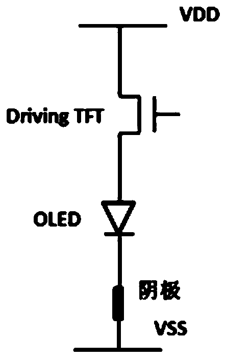
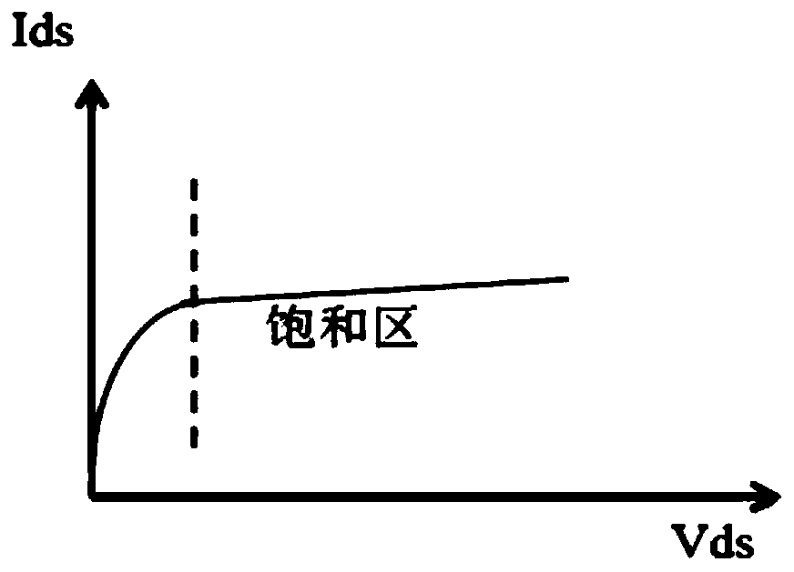
[0035] In organic light emitting diode display panels, such as Figure 1a and Figure 1b As shown, the current flowing through the light emitting structure (such as OLED) is controlled by the driving transistor (Driving TFT). When the voltage difference Vds between the source and drain of the driving transistor reaches a certain value, the driving transistor will work in the saturation region, and the current Ids flowing through the source and drain is only affected by the gate (Gate) voltage. However, in actual situations, the drive transistor will also be affected by other factors (such as channel modulation effects, etc.), so that even in the saturation region, the current I flowing through the source and drain ds is ...


PUM


Abstract

The invention provides a display substrate and a manufacturing method thereof, and a display panel. The problem that the display performance of the existing light-emitting diode display substrate canbe influenced when improving the brightness nonuniformity can be partially solved. The display substrate comprises a substrate; multiple sub-pixels arranged at intervals, wherein an interval region isformed between adjacent sub-pixels; a second electrode layer formed by connecting second electrodes of various sub-pixels as an integer, wherein each sub-pixel is orderly provided with a first electrode, a light-emitting layer and a second electrode in superposition on a direction far away from the substrate; an insulated isolation layer located at one side, far away from a light-emitting layer,of the second electrode layer, wherein the isolation layer covers the second electrode, and an opening is formed one at least partial interval region; and an auxiliary conducting layer located at oneside, far away from the second electrode layer, of the isolation layer, wherein the auxiliary conducting layer is connected with the second electrode layer through the opening.

Description

technical field [0001] The invention belongs to the field of display technology, and in particular relates to a display substrate, a manufacturing method thereof, and a display panel. Background technique [0002] Related Art An organic light emitting diode (OLED) display panel includes sub-pixels distributed in an array, wherein each sub-pixel includes a light-emitting layer, an anode under the light-emitting layer, and a cathode on the light-emitting layer, and the cathodes of each sub-pixel are connected to each other to form a An integral cathode layer, the drive circuit is connected to the cathode layer to provide cathode voltage for the cathode layer (that is, the cathode of each sub-pixel). The organic light emitting diode display panel adopts a top emission method, and the cathode layer further includes an auxiliary luminescent layer (CPL, Capping Layer) covering the cathode layer for improving light extraction rate. [0003] However, the distance between each sub-p...

Claims


Application Information

Patent Timeline
Patent Type & Authority Applications(China)
IPC IPC(8): H01L27/32H01L51/52
CPCH10K59/00H10K59/122H10K50/824H10K71/00H10K59/1201H10K2102/102H10K2102/103H10K2102/351
Inventor 张伟陈龙杨一帆曹鹏曾诚高营昌
Owner BOE TECH GRP CO LTD
Why Eureka
Try Eureka