A vacuum packaging process

A vacuum packaging and process technology, which is applied in decorative arts, processes for producing decorative surface effects, metal material coating processes, etc. Expensive, etc.

Active Publication Date: 2021-05-14
SHANGHAI INST OF MICROSYSTEM & INFORMATION TECH CHINESE ACAD OF SCI
View PDF9 Cites 0 Cited by
  • Summary
  • Abstract
  • Description
  • Claims
  • Application Information

AI Technical Summary

Problems solved by technology

[0010] In order to solve the problem that the high-temperature getter used in the bonding technology in the prior art is incompatible with the MEMS process, and the low-temperature getter is inefficient and expensive, the present invention aims to provide a vacuum packaging process

Method used


Image

  • A vacuum packaging process
  • A vacuum packaging process
  • A vacuum packaging process

Examples


Embodiment Construction

[0030] Below in conjunction with the drawings, preferred embodiments of the present invention are given and described in detail.

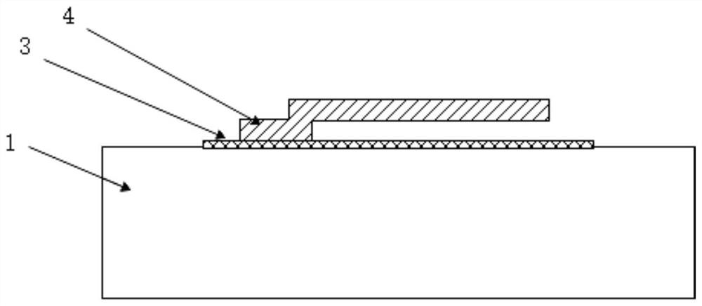
[0031] The vacuum encapsulation process according to the present invention includes: fabricating structures or devices requiring vacuum encapsulation on silicon wafers or glass wafers. According to a preferred embodiment of the present invention, a sensitive movable structure 4 is made on a silicon wafer 1, which is connected to the silicon wafer 1 through an insulating layer 3, such as figure 1 shown. The sensitive movable structure 4 can be fabricated by using conventional MEMS technology, and will not be repeated here. It should be understood that the insulating layer 3 can also be omitted.

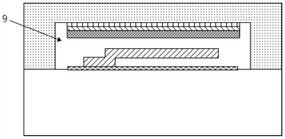
[0032] The vacuum packaging process according to the present invention includes: making an open groove on a glass wafer or a silicon wafer and a metal layer located in the groove. In the present embodiment, groove 5 is made on glass wafer 2, as figure ...


PUM


Abstract

The invention relates to a vacuum encapsulation process, comprising the following steps: providing a silicon wafer and a glass wafer; fabricating a structure or device requiring vacuum encapsulation on one of the silicon wafer and the glass wafer; Open grooves are made on the other of the chips, and a metal layer for local oxidation is made in the grooves; the silicon wafer and the glass wafer are bonded by anodic to form a microcavity structure, which has a structure consisting of The airtight cavity formed by the groove, the metal layer is located inside the airtight cavity, the oxygen generated by the anode bonding enters the inside of the airtight cavity; the radio frequency excites the oxygen inside the airtight cavity to form oxygen plasma, and the metal layer and the oxygen plasma Oxidation reaction occurs in the body to continue to consume oxygen until the oxygen can no longer be ignited to form oxygen plasma. The vacuum encapsulation process provided by the present invention utilizes silicon-glass anode bonding to generate oxygen and the characteristics of continuous oxidation of metal films in oxygen plasma to finally realize vacuum encapsulation.

Description

technical field [0001] The invention relates to micro-nano processing technology, and more specifically relates to a vacuum packaging process. Background technique [0002] Air resistance is a force that is proportional to the size of the structure. In macroscopic objects, air resistance only has a significant effect when the velocity is high. But the relative influence of air resistance increases significantly as the size of the structure decreases. In common micro-scale microelectromechanical systems (MEMS) structures, air resistance is the main damping mechanism for many MEMS devices. At the same time, according to the Langevin equation, in order to achieve thermal equilibrium damping, noise must be caused, and air damping is also the main noise mechanism of various MEMS devices. Therefore, vacuum packaging is one of the key technologies for various MEMS devices. [0003] The air damping of MEMS devices is generally characterized by the Q value of the device. Accordi...

Claims


Application Information

Patent Timeline
Patent Type & Authority Patents(China)
IPC IPC(8): B81C1/00B81B7/00
Inventor 裴彬彬孙珂杨恒豆传国李昕欣
Owner SHANGHAI INST OF MICROSYSTEM & INFORMATION TECH CHINESE ACAD OF SCI
Why Eureka
Try Eureka