
A kind of p-type algan material with high mobility and high hole concentration and its growth method

A technology with high hole concentration and high mobility, which is applied in semiconductor devices, electrical components, circuits, etc., can solve the problems of low mobility and low hole concentration of P-type AlGaN, achieve remarkable effects, simple process, and broad application prospects Effect

Active Publication Date: 2020-04-03
CHANGCHUN INST OF OPTICS FINE MECHANICS & PHYSICS CHINESE ACAD OF SCI
View PDF10 Cites 0 Cited by
  • Summary
  • Abstract
  • Description
  • Claims
  • Application Information

AI Technical Summary

Problems solved by technology

[0006] In order to solve the problems of low mobility and low hole concentration of P-type AlGaN in the prior art, the present invention provides a P-type AlGaN material with high mobility and high hole concentration and a growth method thereof

Method used


Image

  • A kind of p-type algan material with high mobility and high hole concentration and its growth method
  • A kind of p-type algan material with high mobility and high hole concentration and its growth method

Examples


Embodiment Construction

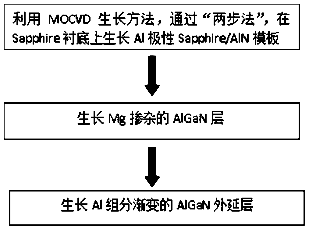
[0032] Further illustrate the present invention below in conjunction with accompanying drawing.

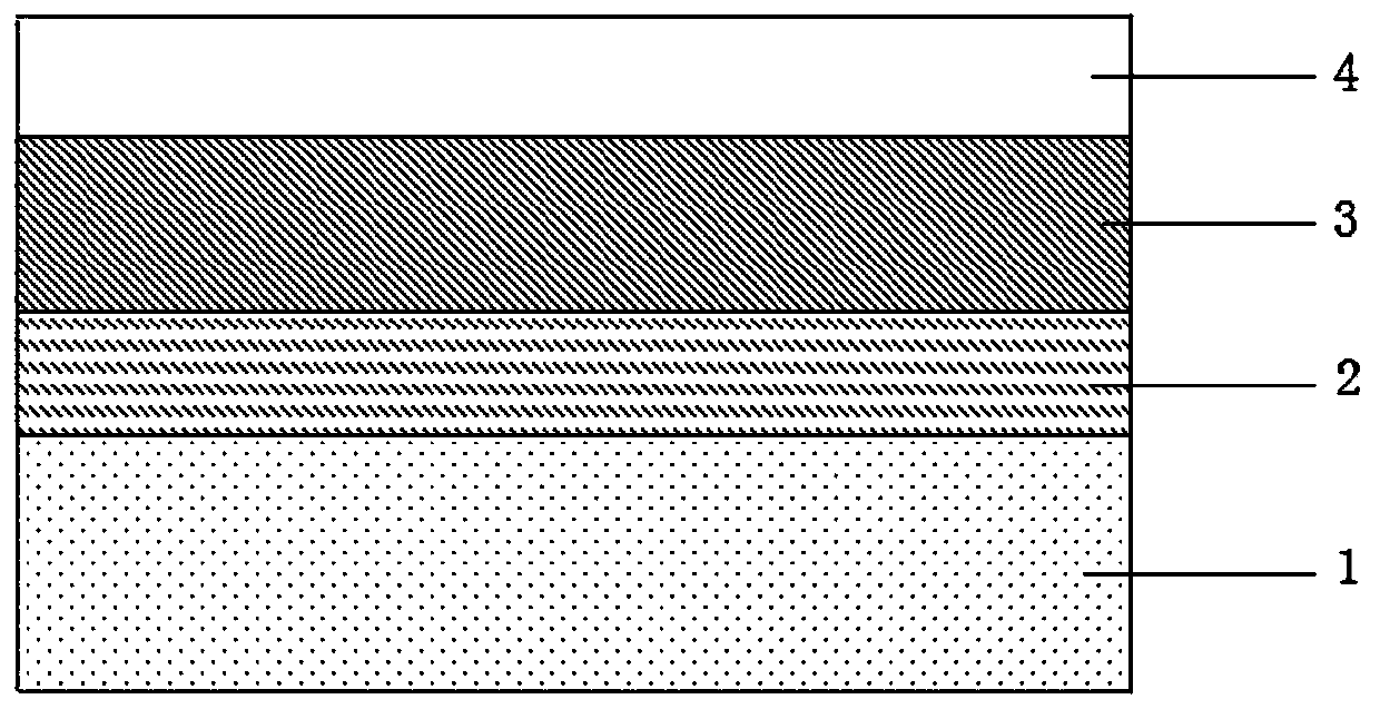
[0033] Such as figure 1 As shown, the high mobility and high hole concentration P-type AlGaN material of the present invention includes an aluminum nitride layer 2, a doped epitaxial layer 3 and a graded epitaxial layer 4 arranged in sequence from bottom to top, and may also include an aluminum nitride layer 2 Substrate layer 1 on the lower surface.

[0034] Wherein, the material of the substrate layer 1 is commonly used substrate materials such as sapphire, silicon carbide, and silicon.

[0035] The aluminum nitride layer 2 is an Al polar surface, and its thickness is preferably 1-5 μm.

[0036] The material of the doped epitaxial layer 3 is Mg-doped AlGaN, and the doping concentration is not particularly limited, and can be selected according to actual needs; the doped epitaxial layer 3 is metal surface polarity; the thickness is preferably greater than 0 and less than 1.5 μm....


PUM

PropertyMeasurementUnit
thicknessaaaaaaaaaa
thicknessaaaaaaaaaa
thicknessaaaaaaaaaa

Abstract

The invention relates to a P-type AlGaN material with high mobility and high hole concentration and a growth method thereof, belonging to the technical field of semiconductors. The problems of low mobility and low hole concentration of P-type AlGaN in the prior art are solved. The P-type AlGaN material of the present invention includes an aluminum nitride layer, a doped epitaxial layer and a graded epitaxial layer arranged in sequence from bottom to top; the aluminum nitride layer is an Al polar plane; the material of the doped epitaxial layer is Mg-doped P-type AlGaN, the doped epitaxial layer is the polarity of the metal surface; the graded epitaxial layer is a multi-layer structure arranged from bottom to top, and each layer of material is unintentionally doped with Al x Ga 1‑x N material, and multi-layer unintentionally doped Al x Ga 1‑x The Al composition of the N material decreases gradually from bottom to top. The P-type AlGaN material is based on the idea that the polarization-induced charge simultaneously separates the carrier migration region and the impurity ionization region to achieve high mobility and high hole concentration.

Description

technical field [0001] The invention belongs to the technical field of semiconductors, and in particular relates to a P-type AlGaN material with high mobility and high hole concentration and a growth method thereof. Background technique [0002] As a III-V ternary alloy material, AlGaN's forbidden band width is continuously adjustable between 3.4-6.2eV with the change of Al composition from low to high, corresponding to the deep ultraviolet range from 365nm to 200nm. AlGaN materials have unique advantages such as radiation resistance and easy wavelength adjustment. It is an ideal material for preparing ultraviolet and deep ultraviolet optoelectronic devices. [0003] The application basis of semiconductor devices is the PN junction, and the realization of high-conductivity P-type and N-type is the prerequisite for AlGaN materials to achieve specific functions and be applied to practical devices. For AlGaN materials, due to the existence of intrinsic defects and donor impur...

Claims


Application Information

Patent Timeline
Patent Type & Authority Patents(China)
IPC IPC(8): H01L29/20H01L21/02
CPCH01L21/0242H01L21/0254H01L21/02579H01L21/0262H01L29/2003
Inventor 黎大兵蒋科孙晓娟贾玉萍石芝铭刘贺男
Owner CHANGCHUN INST OF OPTICS FINE MECHANICS & PHYSICS CHINESE ACAD OF SCI
Learn More