A kind of algan-based ultraviolet heterojunction phototransistor detector and its preparation method
A phototransistor and detector technology, applied in semiconductor devices, circuits, electrical components, etc., can solve the problems of uncertainty in the thickness of the main doping region, and the device structure does not meet the design requirements, so as to eliminate adverse effects and ensure reliable device operation. Performance, effect of high epitaxial crystal quality
- Summary
- Abstract
- Description
- Claims
- Application Information
AI Technical Summary
Problems solved by technology
Method used
Image
Examples
Embodiment 1
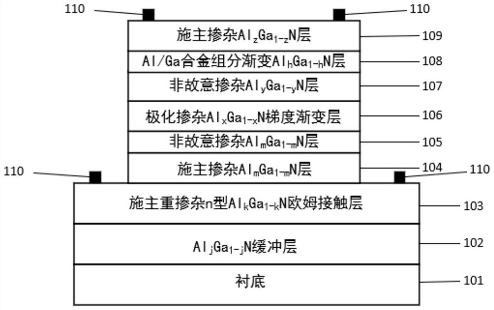
[0042] An AlGaN-based ultraviolet heterojunction phototransistor detector, such as figure 1 As shown, it is an npn-type structure, and the p-type base region is grown by polarized doping. The phototransistor detector includes a substrate 101 and an epitaxial layer grown on the substrate 101. The epitaxial layer includes sequentially from bottom to top Distributed buffer layer 102, n-type ohmic contact layer 103, donor-doped Al m Ga 1-m N layer 104, unintentionally doped with Al m Ga 1-m N layer 105, polarized doped p-type Al x Ga 1-x N gradient layer 106, Al y Ga 1-y N layer 107, Al with graded Al / Ga composition h Ga 1-h N layer 108, Al z Ga 1-z N layer 109 and distributed in ohmic contact layer 103 and Al z Ga 1-z The n-type ohmic contact electrode 110 on the N layer 109, wherein the starting value of the Al composition x≤m-0.1, and the ending value is y; m-0.4≤y≤m-0.2; the starting value of h is y, and the ending value is is z; y+0.1≤z≤y+0.2.
[0043] The prese...
Embodiment 2
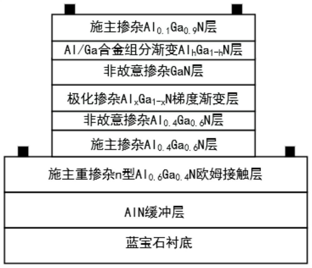
[0062] A kind of AlGaN-based ultraviolet heterojunction phototransistor detector described in this embodiment, such as figure 2 As shown, the npn structure is adopted, and the p-type base region is grown by polarized doping to provide the required carriers (holes). The phototransistor detector includes a c-plane sapphire substrate and an epitaxial layer, and the epitaxial The layer structure includes an AlN buffer layer with a thickness of 0.5 μm; a donor heavily doped n-type Al with a thickness of 1 μm 0.6 Ga 0.4N ohmic contact layer with an electron concentration of 3.5×10 18 cm -3 ; Donor-doped Al with a thickness of 100 nm 0.4 Ga 0.6 N layer with electron concentration of 1×10 18 cm -3 ; Thickness 10nm unintentionally doped Al 0.4 Ga 0.6 N layer; thickness 100nm polarized doped Al x Ga 1-x In the N gradient layer, the Al component is grown by a linear gradient, from a high Al component to a low Al component, and the Al component x=0.3~0, and the measured hole co...
Embodiment 3
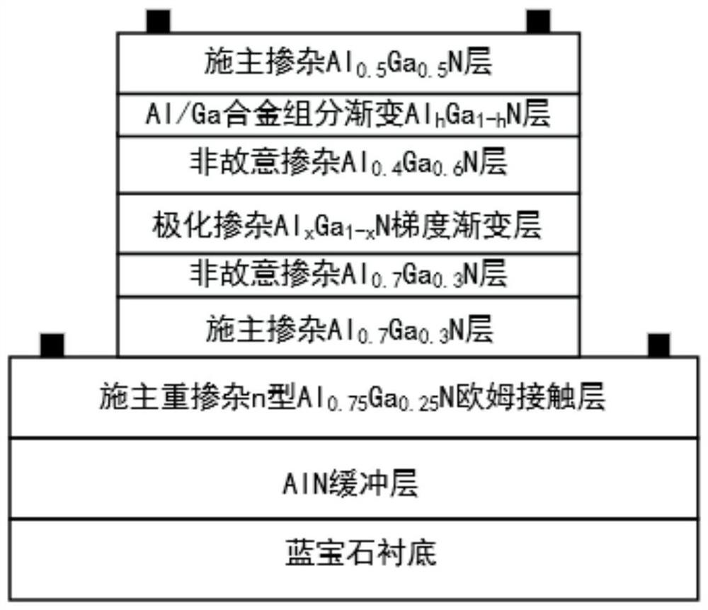
[0072] The phototransistor detector described in this embodiment is an AlGaN-based sun-blind ultraviolet heterojunction phototransistor, and its preparation method is basically the same as that of Example 1, the difference being that, as image 3 As shown, the structure of the epitaxial layer includes an AlN buffer layer with a thickness of 0.5 μm; a donor heavily doped n-type Al layer with a thickness of 1 μm 0.75 Ga 0.25 N ohmic contact layer with an electron concentration of 3.5×10 18 cm -3 ; Donor-doped Al with a thickness of 100 nm 0.7 Ga 0.3 N layer with electron concentration of 1×10 18 cm -3 ; Thickness 10nm unintentionally doped Al 0.7 Ga 0.3 N layer; thickness 100nm polarized doped Al x Ga 1-x In the N gradient layer, the Al component is grown by a linear gradient, from a high Al component to a low Al component, and the Al component x=0.7~0.4, and the measured hole concentration under the coherent growth condition is 3.6× 10 18 cm -3 ; Unintentionally dop...
PUM
| Property | Measurement | Unit |
|---|---|---|
| thickness | aaaaa | aaaaa |
| thickness | aaaaa | aaaaa |
| thickness | aaaaa | aaaaa |
Abstract
Description
Claims
Application Information
 - Generate Ideas
- Intellectual Property
- Life Sciences
- Materials
- Tech Scout
- Unparalleled Data Quality
- Higher Quality Content
- 60% Fewer Hallucinations
Browse by: Latest US Patents, China's latest patents, Technical Efficacy Thesaurus, Application Domain, Technology Topic, Popular Technical Reports.
© 2025 PatSnap. All rights reserved.Legal|Privacy policy|Modern Slavery Act Transparency Statement|Sitemap|About US| Contact US: help@patsnap.com


