Array substrate, display panel and display device
An array substrate and display panel technology, which is applied in electrical components, electric solid state devices, circuits, etc., can solve the problems of low resolution, low material utilization rate, and high material utilization rate of display panel products.
- Summary
- Abstract
- Description
- Claims
- Application Information
AI Technical Summary
Problems solved by technology
Method used
Image
Examples
Embodiment 1
[0029] The array substrate provided by the embodiment of the present invention includes:
[0030] Substrate (not shown in the figure);
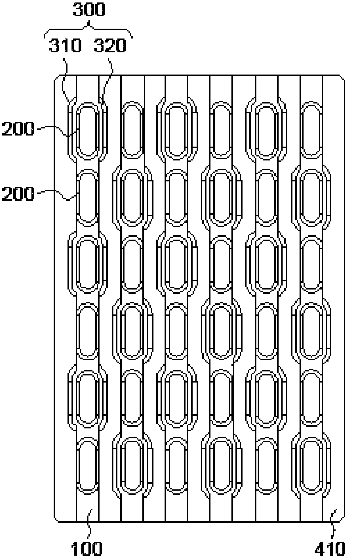
[0031] The pixel defining layer formed on the substrate, the pixel defining layer includes a plate body 400, the surface of the plate body 400 facing away from the substrate is the first surface, and the surface of the plate body 400 facing the substrate is the second surface, the plate body 400 has an opening A plurality of channels 100 located on the first surface, a plurality of pixel pits 200 are formed at the bottom of each channel 100; each channel 100 has opposite first sidewalls and second sidewalls, and the first sidewall is provided with a plurality of The opening faces the first recess 310 of the second side wall, and the second side wall is provided with a second recess 320 corresponding to the first recess 310 and opening toward the first side wall, each pair of first recesses 310 corresponding to each other It is arranged oppos...
Embodiment 2
[0054] The display panel provided by the embodiment of the present invention includes: the array substrate provided by the first embodiment.
[0055] The display panel includes the array substrate provided in Embodiment 1, the array substrate includes a pixel defining layer formed on the substrate, the pixel defining layer includes a board body 400, and the board body 400 has a plurality of channels 100 with openings located on the first surface, each A plurality of pixel pits 200 are formed at the bottom of the channel 100, and the first depression 310 on the first side wall of the channel 100 and the second depression 320 on the second side wall of the channel 100 form the craters 300 in one-to-one correspondence; inkjet printing is performed on the array substrate At this time, the print nozzle is aimed at the crater 300 to drop ink, and the ink enters the channel 100 from the crater 300, and flows to each pixel hole 200 along the channel 100 to complete the printing of each...
Embodiment 3
[0057] The display device provided by the embodiment of the present invention includes: the display panel provided by the third embodiment.
[0058] The array substrate in the display device includes a pixel defining layer formed on the substrate. The pixel defining layer includes a plate body 400. The plate body 400 has a plurality of channels 100 with openings located on the first surface. A plurality of channels 100 are formed at the bottom of each channel 100. The pixel crater 200, the first depression 310 on the first side wall of the channel 100, and the second depression 320 on the second side wall form the bullet crater 300 in one-to-one correspondence; when inkjet printing is performed on the array substrate, the print head is aligned with the There are 300 drops of ink in the crater, and the ink enters the channel 100 by the crater 300, and flows to each pixel crater 200 along the channel 100, so as to complete the printing of each pixel; Compared with directly dropp...
PUM
 Abstract
Description
Claims
Application Information
 - R&D Engineer
- R&D Manager
- IP Professional
- Industry Leading Data Capabilities
- Powerful AI technology
- Patent DNA Extraction
Browse by: Latest US Patents, China's latest patents, Technical Efficacy Thesaurus, Application Domain, Technology Topic, Popular Technical Reports.
© 2024 PatSnap. All rights reserved.Legal|Privacy policy|Modern Slavery Act Transparency Statement|Sitemap|About US| Contact US: help@patsnap.com


