Pixel circuit, driving method thereof and display panel
A pixel circuit and drive unit technology, applied in static indicators, instruments, etc., can solve problems such as threshold voltage drift, abnormal display, etc., and achieve the effect of improving service life and display effect
- Summary
- Abstract
- Description
- Claims
- Application Information
AI Technical Summary
Problems solved by technology
Method used
Image
Examples
Embodiment 1
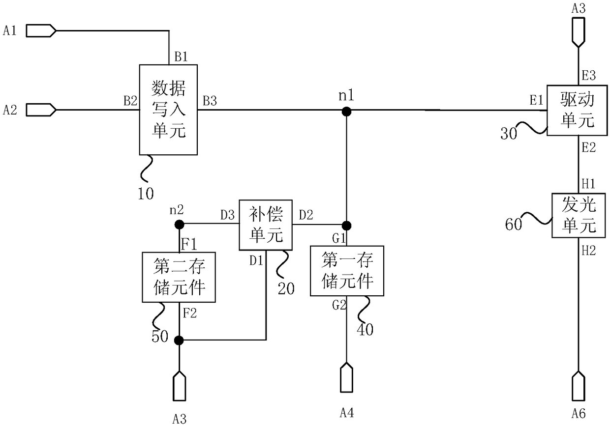
[0044] figure 1 A schematic structural diagram of a pixel circuit provided in Embodiment 1 of the present invention, as shown in figure 1 As shown, the pixel circuit includes a data writing unit 10 , a compensation unit 20 , a driving unit 30 , a first storage element 40 and a second storage element 50 .
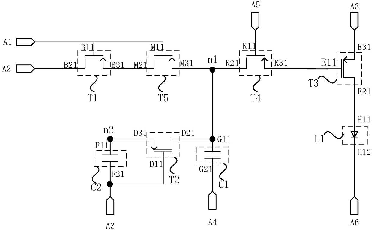
[0045]Wherein, the control terminal B1 of the data writing unit 10 is connected to the scan signal input terminal A1 of the pixel circuit, the first terminal B2 is connected to the data signal input terminal A2 of the pixel circuit, and the second terminal B3 is connected to the first node n1. The control terminal D1 of the compensation unit 20 is connected to the first level signal input terminal A3 of the pixel circuit, and the first terminal D2 is connected to the first node n1. The control terminal E1 of the driving unit 30 is connected to the first node n1, the first terminal E2 is connected to the first electrode H1 of the light emitting element 60, and the second ter...
Embodiment 2
[0082] On the basis of the above embodiments, Embodiment 2 of the present invention provides a display panel, Figure 4 It is a schematic structural diagram of a display panel provided by an embodiment of the present invention. Such as Figure 4 As shown, the display panel 200 includes the pixel circuit 100 of the above embodiment. The display panel 200 may include a plurality of light emitting elements 60 arranged in a matrix. Each pixel circuit 100 is set corresponding to a light emitting element 60 in the display panel 200. The light emitting element 60 is arranged in a Under the action of the driving current generated by the pixel circuit 100, light-emitting display is performed. Figure 4 Only one thin film transistor is used as an example to represent one pixel circuit 100, and the pixel circuit 100 also includes other thin film transistors and storage capacitors.
[0083] Since the second embodiment of the present invention includes the pixel circuit of the above-ment...
Embodiment 3
[0085] On the basis of the above examples, Figure 5 It is a schematic flow chart of a pixel circuit driving method provided by Embodiment 3 of the present invention. The technical solution of this embodiment can be applied in a scene where pixel circuits need to be driven, and can be executed by the pixel circuit provided by the embodiment of the present invention. The method includes:
[0086] S110, the data signal writing phase, the data writing unit and the compensation unit are turned on, and the driving unit is turned off; the data signal is written into the first node through the data writing unit, and written into the second node through the data writing unit and the compensation unit.
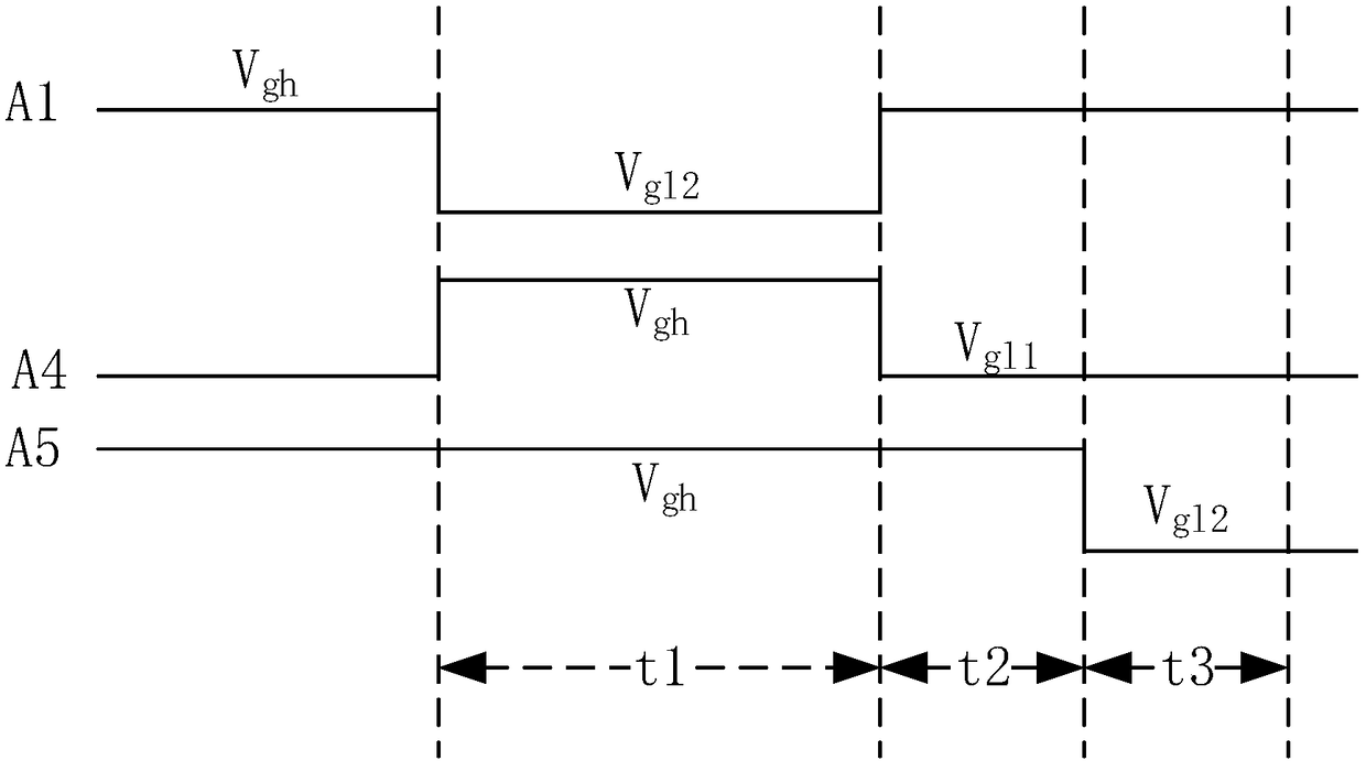
[0087] Exemplary, combined with figure 2 and image 3 , can control the first thin film transistor T1 and the second thin film transistor T2 to turn on, the third thin film transistor T3 to turn off, the data signal is written into the first node n1 through the first thin film trans...
PUM
 Abstract
Description
Claims
Application Information
 - Generate Ideas
- Intellectual Property
- Life Sciences
- Materials
- Tech Scout
- Unparalleled Data Quality
- Higher Quality Content
- 60% Fewer Hallucinations
Browse by: Latest US Patents, China's latest patents, Technical Efficacy Thesaurus, Application Domain, Technology Topic, Popular Technical Reports.
© 2025 PatSnap. All rights reserved.Legal|Privacy policy|Modern Slavery Act Transparency Statement|Sitemap|About US| Contact US: help@patsnap.com


