Making method of PCB and PCB
A manufacturing method and a part of the technology, which are used in the manufacture of printed circuits, the formation of electrical connections of printed components, and electrical components, can solve problems such as limiting density, difficult drilling of metal blocks, affecting heat dissipation performance, and grounding shielding performance, so as to meet the design requirements. requirements, avoiding the effect of reducing the pore density
- Summary
- Abstract
- Description
- Claims
- Application Information
AI Technical Summary
Problems solved by technology
Method used
Image
Examples
Embodiment 1
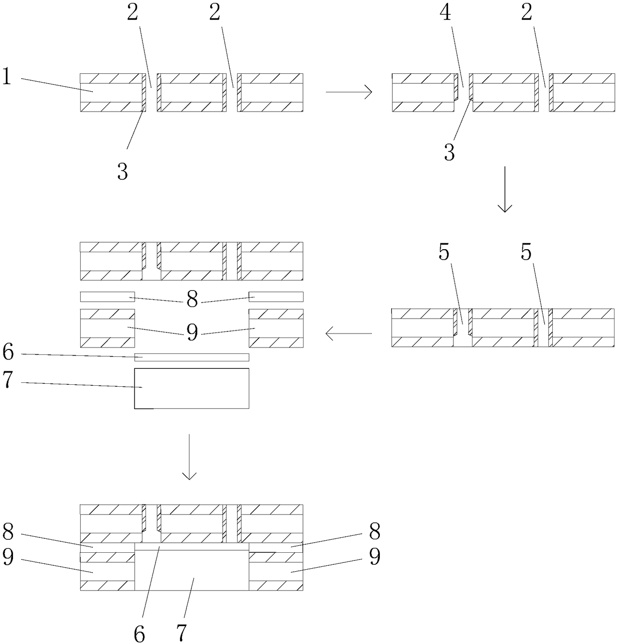
[0063] This embodiment provides a method for manufacturing a PCB, which can be used to manufacture a PCB with a metal block or a metal base. The metal block includes a ground hole and a signal hole with a metalized hole wall. The ground hole is connected to the metal block, and the signal hole is connected to the metal. The block is insulated, and each hole can be made with a smaller aperture to increase the hole density and achieve a good grounding and heat dissipation effect.
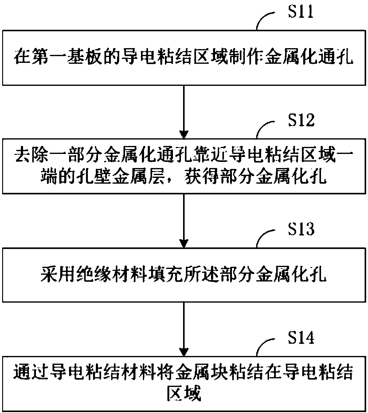
[0064] figure 1 It is a flowchart of the manufacturing method of the PCB in this embodiment. Such as figure 1 As shown, the manufacturing method includes the following steps:
[0065] S11, forming a metalized through hole in the conductive bonding area of the first substrate.
[0066] A single core board or multiple core boards are laminated as the first substrate. According to the structural design requirements of the PCB, the area where the conductive metal block needs to be bonded is the conductive bon...
Embodiment 2
[0078] In this embodiment, on the basis of the above embodiment, the metal block is buried. figure 2 It is a flowchart of the manufacturing method of the PCB in this embodiment. Such as figure 2 As shown, the manufacturing method of this embodiment includes the following steps:
[0079] S21, making metallized through holes in the conductive bonding area of the first substrate.
[0080] S22, removing a part of the metal layer of the hole wall of the metalized through hole near one end of the conductive bonding area to obtain a part of the metalized hole.
[0081] S23, using an insulating material to fill the partially metalized hole.
[0082] S24, providing a second substrate and a first prepreg, and opening slots on the second substrate and the first prepreg at positions corresponding to the conductive bonding area according to the size of the metal block.
[0083] The sum of the thickness of the second substrate and the first prepreg is equal to the sum of the thickness of the met...
Embodiment 3
[0092] In this embodiment, on the basis of the first embodiment, if the metal block is designed as an exposed metal block, auxiliary facilities need to be provided during pressing. Figure 4 It is a flowchart of the manufacturing method of the PCB in this embodiment. Such as Figure 4 As shown, the manufacturing method of this embodiment includes the following steps:
[0093] S31, forming a metalized through hole in the conductive bonding area of the first substrate.
[0094] S32, removing a part of the hole wall metal layer of the metalized through hole near one end of the conductive bonding area to obtain a part of the metalized hole.
[0095] S33, filling the part of the metallized holes with an insulating material.
[0096] In this embodiment, the metal block is exposed. If the surface treatment and shape production are performed after the metal block is bonded, the metal block will be damaged. Therefore, the first substrate needs to be surface treated before bonding the metal b...
PUM
 Abstract
Description
Claims
Application Information
 - R&D Engineer
- R&D Manager
- IP Professional
- Industry Leading Data Capabilities
- Powerful AI technology
- Patent DNA Extraction
Browse by: Latest US Patents, China's latest patents, Technical Efficacy Thesaurus, Application Domain, Technology Topic, Popular Technical Reports.
© 2024 PatSnap. All rights reserved.Legal|Privacy policy|Modern Slavery Act Transparency Statement|Sitemap|About US| Contact US: help@patsnap.com


