Circuit board defect tracking method, device and computer equipment based on positioning holes

A technology for positioning holes and circuit boards, applied in computer-aided design, circuit board tool positioning, calculation, etc., can solve problems such as error-prone, affect the efficiency of defect tracking process, time-consuming and labor-intensive, and achieve the effect of improving efficiency

Active Publication Date: 2021-04-06
GUANGZHOU FASTPRINT CIRCUIT TECH +2
View PDF6 Cites 0 Cited by
  • Summary
  • Abstract
  • Description
  • Claims
  • Application Information

AI Technical Summary

Problems solved by technology

In the process of realizing the present invention, the inventor found that there are at least the following problems in the prior art: at present, the production and format modification of drilling files are mainly completed manually by CAM engineers, but manual modification is not only time-consuming and labor-intensive, but also prone to errors, reducing positioning The speed at which holes are generated can affect the efficiency of the defect tracking process

Method used


Image

  • Circuit board defect tracking method, device and computer equipment based on positioning holes
  • Circuit board defect tracking method, device and computer equipment based on positioning holes
  • Circuit board defect tracking method, device and computer equipment based on positioning holes

Examples


Embodiment Construction

[0022] In order to make the object, technical solution and advantages of the present invention clearer, the present invention will be further described in detail below in conjunction with the accompanying drawings and embodiments. It should be understood that the specific embodiments described here are only used to explain the present invention, not to limit the present invention.

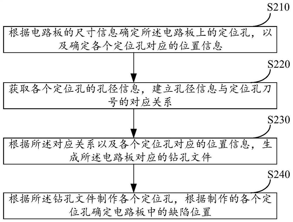
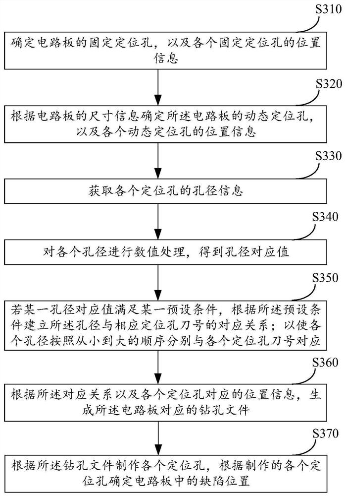
[0023] At present, when the Defect Mapping system tracks the location information of defective units, the management of the lot unit panel number (panel) is changed to the defects of the panel number (panel), strip number (strip) and unit (PCS unit) In this way, the defect location can be directly tracked to the unit, which greatly improves the accuracy and effectiveness of defect tracking. CAM engineers need to create center file drilling files for each type of circuit board, and make the machine automatically align and find out the printing position according to the coordinates of the positioning...


PUM


Abstract

The invention relates to a circuit board defect tracking method, device and computer equipment based on positioning holes, and belongs to the technical field of electronic circuits. The method includes: determining the positioning holes on the circuit board according to the size information of the circuit board, and determining the position information corresponding to each positioning hole; obtaining the aperture information of each positioning hole, and establishing the corresponding relationship between the aperture information and the positioning hole cutter number ; According to the corresponding relationship and the position information corresponding to each positioning hole, generate the drilling file corresponding to the circuit board; generate the corresponding virtual positioning hole on the circuit board according to the drilling file, and determine according to the virtual positioning hole Defect location in circuit board. The above technical solution solves the problem of low defect tracking efficiency due to manual modification of drilling files, and can automatically control equipment to generate positioning holes according to the actual situation of the circuit board, improving the efficiency of circuit board defect tracking.

Description

technical field [0001] The invention relates to the technical field of electronic circuits, in particular to a circuit board defect tracking method, device, computer equipment and storage medium based on positioning holes. Background technique [0002] Defect Mapping (defect scrapping traceability system) can track the location information of circuit board defect units. Defect information includes panel number (panel), strip number (strip / set), unit (PCS unit), and defect location can be traced directly to unit , with high accuracy and effectiveness. Before defect tracking, CAM (Computer Aided Manufacturing, computer-aided manufacturing) engineers need to create a center file drilling file (center alignment file, referred to as center file or drilling file) for each production model pnl (abbreviation of panel) file . The machine can automatically align and find out the printing position of the positioning hole according to the coordinates of the drilling file. In the proc...

Claims


Application Information

Patent Timeline
Patent Type & Authority Patents(China)
IPC IPC(8): G06F30/398G01B21/02G01B21/10G01R31/28
CPCG01B21/02G01B21/10G01R31/2801G06F30/392G06F30/398H05K3/0047H05K3/0008H05K2201/09063H05K2201/09918
Inventor 钟利东何欢谢添华江武骏
Owner GUANGZHOU FASTPRINT CIRCUIT TECH
Why Eureka
Try Eureka