A semiconductor tube protection circuit and method
A semiconductor tube and protection circuit technology, which is applied in the field of semiconductor tube protection circuits, can solve the problems of MOS tubes lacking circuit overload capacity, MOS tubes are easy to be broken down, etc., and achieve the effect of protecting against breakdown and increasing the pressure resistance
- Summary
- Abstract
- Description
- Claims
- Application Information
AI Technical Summary
Problems solved by technology
Method used
Image

Examples
Embodiment 1
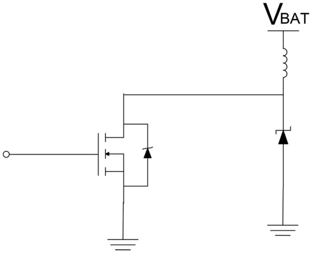
[0045] When the switch of the MOS tube is controlled by the relay, the MOS tube drives the inductive load. Due to the instantaneous opening of the relay, the dV / dt is too large, that is, the instantaneous change of the voltage is too large, so that the voltage change rate accumulated on the MOS tube is too fast, causing the parasitic transistor of the MOS tube to break down.
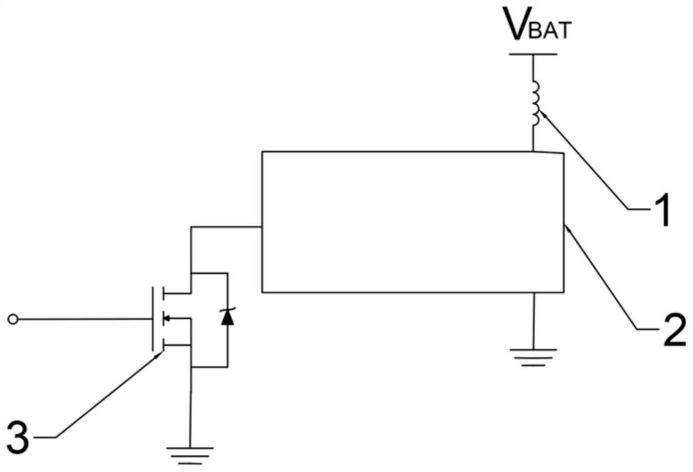
[0046] Such as figure 2 As shown, it is an existing MOS tube protection circuit.
[0047] When the relay is turned off, due to the start-up period of the relay, a huge transient voltage (dV / dt) will be generated, forming a huge surge phenomenon. Since the MOS tube just drives the inductive load, this high transient voltage will activate the MOS The parasitic transistor contained in the tube (the diode connected between the drain of the MOS tube and the source of the MOS tube, when a large instantaneous reverse current is generated in the circuit, it can be derived through this diode, protecting the MOS...
Embodiment 2
[0068] Based on embodiment 1, the difference from embodiment 1 is:
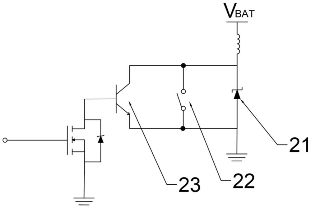
[0069] Such as figure 1 with Figure 4 Shown is a circuit diagram of a semiconductor tube protection circuit of the present invention.
[0070] Since the power supply voltage of the circuit is different in different application scenarios, in order to adapt to more different power supply voltages, the Zener diode 21 in Embodiment 1 is improved into a voltage stabilizing unit 24 .
[0071] The voltage stabilizing circuit 2 includes a voltage stabilizing unit 24 and the relay 22 .
[0072] The voltage stabilizing unit 24 is connected in parallel with the relay 22 .
[0073] The high potential end of the voltage stabilizing unit 24 is connected to the low potential end of the load unit 1 , and the low potential end of the voltage stabilizing unit 24 is grounded.
[0074] The voltage stabilizing unit 24 includes at least two voltage stabilizing subunits 241 connected in series. The voltage stabilizing subunit ...
Embodiment 3
[0079] Based on Embodiment 1, this embodiment is a design method corresponding to Embodiment 1.
[0080] Such as Figure 5 As shown, it is a flow chart of a semiconductor tube protection method corresponding to Embodiment 1.
[0081] A semiconductor tube protection method, comprising:
[0082] S1, adding the voltage-zener diode 21 in the circuit to divert current, and divert most of the instantaneous voltage generated after the relay is turned on to the system ground.
[0083] The Zener diode 21 works by utilizing the property that the breakdown region of the PN junction has a stable voltage. The characteristic of the Zener diode is that after breakdown, the voltage at both ends remains basically unchanged. In this way, when the Zener tube is connected to the circuit, if the voltage of each point in the circuit changes due to fluctuations in the power supply voltage or other reasons, the voltage at both ends of the load will remain basically unchanged. After the reverse br...
PUM
 Abstract
Description
Claims
Application Information
 - Generate Ideas
- Intellectual Property
- Life Sciences
- Materials
- Tech Scout
- Unparalleled Data Quality
- Higher Quality Content
- 60% Fewer Hallucinations
Browse by: Latest US Patents, China's latest patents, Technical Efficacy Thesaurus, Application Domain, Technology Topic, Popular Technical Reports.
© 2025 PatSnap. All rights reserved.Legal|Privacy policy|Modern Slavery Act Transparency Statement|Sitemap|About US| Contact US: help@patsnap.com