A kind of manufacturing method of LED lamp and LED lamp

A technology of LED lamps and manufacturing methods, which is applied in the direction of semiconductor devices, electrical components, circuits, etc., and can solve the problems of LED wafer arrangement or shape restrictions, uneven light, etc.

Active Publication Date: 2019-11-08
常州市弗莱蒙特智能科技有限公司
View PDF8 Cites 0 Cited by
  • Summary
  • Abstract
  • Description
  • Claims
  • Application Information

AI Technical Summary

Problems solved by technology

However, in general, for the convenience of bonding, the bonding pads of the positive and negative poles in the LED wafer 1 are arranged on the side of the LED wafer that emits light outwards, and are used to connect the positive and negative poles of the LED wafer 1 to the receiving end. The wire 4 electrically connected to the positive and negative electrodes on the seat 2 will block the LED wafer 1, making the light emitted by the LED wafer 1 uneven
In addition, the substrate or socket will impose certain restrictions on the arrangement or shape of the LED wafer

Method used


Image

  • A kind of manufacturing method of LED lamp and LED lamp
  • A kind of manufacturing method of LED lamp and LED lamp
  • A kind of manufacturing method of LED lamp and LED lamp

Examples


Embodiment 1

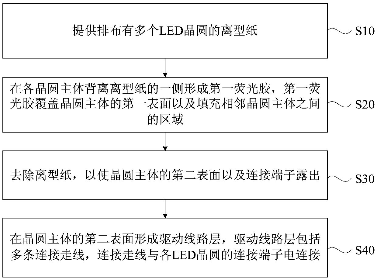
[0042] figure 2 It is a method for manufacturing an LED lamp provided in Embodiment 1 of the present invention. Figure 3-Figure 6 is to use figure 2 The LED light manufacturing method provided in the LED light is a structural schematic diagram of each state of the LED light when making an LED light. see figure 2 and Figure 3-Figure 6 , the manufacturing method of the LED lamp, comprising:

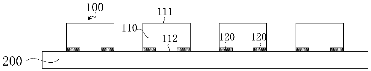
[0043] S10, providing a release paper on which a plurality of LED wafers are arranged.

[0044] see image 3 , providing a release paper 200 on which a plurality of LED wafers 100 are arranged. The LED wafer 100 includes a wafer body 110 and at least two connection terminals 120. The surface of the wafer body 110 away from the release paper 200 is the first surface 111, and the surface of the wafer body 110 close to the release paper 200 is the second surface 112. , at least two connection terminals 120 are disposed on the second surface 112 of the wafer body 110 and are electri...

Embodiment 2

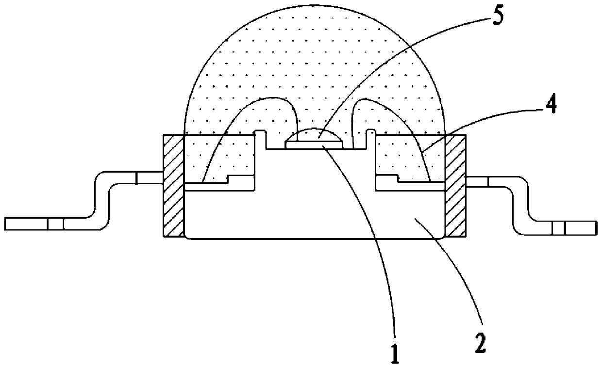
[0064] The embodiment of the present invention also provides an LED lamp, which can be manufactured by using any one of the manufacturing methods of the LED lamp in the above-mentioned embodiments. Figure 7 It is a schematic structural diagram of an LED lamp provided in Embodiment 2 of the present invention. Figure 8 is along Figure 7 Schematic diagram of the cross-sectional structure of A1-A2. see Figure 7 and Figure 8 , the LED lamp 10 includes: a plurality of LED wafers 100, the LED wafer 100 includes a wafer body 110 and at least two connection terminals 120, the wafer body 110 includes a first surface 111 and a second surface 112 oppositely arranged, at least The two connection terminals 120 are arranged on the second surface 112 of the wafer body 110 and are electrically insulated from each other; the first fluorescent glue 300 is formed on the side of each wafer body 110 away from the second surface 112, and the first fluorescent glue 300 covers The first surfa...

Embodiment 3

[0068] Figure 9 It is a schematic cross-sectional structure diagram of an LED lamp provided in Embodiment 3 of the present invention. Compared with the second embodiment, in this embodiment, the LED lamp further includes a phosphor layer. see Figure 9 The phosphor layer 500 is located between the first phosphor glue 300 and the wafer body 110 , covering the first surface 111 of the wafer body 110 and the side surface 113 intersecting the first surface 111 and the second surface 112 . This setting can make the light emitted by the LED wafer 100 pass through the phosphor layer 500 first, and the phosphor layer 500 can initially solidify the color temperature and brightness of various angles, so that the light emitted by the wafer body 110 is more uniform, and avoid the LED wafer. The phenomenon of non-uniform luminescence caused by only covering the first fluorescent glue 300 on the side of the 100 away from the second surface 112 occurs.


PUM


Abstract

The invention provides a manufacturing method of an LED lamp and the LED lamp. The manufacturing method of the LED lamp comprises the steps that release paper on which multiple LED wafers are arrangedis provided, each LED wafer comprises a wafer body and at least two connecting terminals, the water body comprises a first surface and a second surface which are oppositely arranged, and at least twoconnecting terminals are arranged on the second surface of the wafer body and mutually electrically insulated; first fluorescent glue is formed on one side, which is back to the release paper, of each wafer body, and the first fluorescent glue covers the first surface of the wafer body and fills the area between the adjacent wafer bodies; the release paper is removed so that the second surface ofthe wafer body and the connecting terminals are enabled to be exposed; and a driving line layer is formed on the second surface of the wafer body, and the driving line layer comprises multiple connecting wires which are electrically connected with the connecting terminals of each LED wafer. According to the scheme, the LED wafers can be conveniently and flexibly arranged, the effect of great luminance uniformity of the LED lamp can be realized and the performance of the LED lamp can be enhanced.

Description

technical field [0001] Embodiments of the present invention relate to LED lighting technology, in particular to a method for manufacturing an LED lamp and the LED lamp. Background technique [0002] Light Emitting Diodes (LEDs) have the advantages of high transparency, high brightness, long life and good stability, and are widely used in many fields of social life. [0003] figure 1 It is an LED lighting module in the prior art. see figure 1 , usually the LED wafer is placed on the substrate or the socket 2, and the positive and negative electrodes in the LED wafer 1 are welded to the positive and negative electrodes on the socket 2 through the wire 4, so that the LED wafer 1 and the external driver chip connect. However, in general, for the convenience of bonding, the bonding pads of the positive and negative poles in the LED wafer 1 are arranged on the side of the LED wafer that emits light outwards, and are used to connect the positive and negative poles of the LED wa...

Claims


Application Information

Patent Timeline
Patent Type & Authority Patents(China)
IPC IPC(8): H01L33/48H01L33/62H01L33/50
CPCH01L33/48H01L33/50H01L33/62
Inventor 包锋
Owner 常州市弗莱蒙特智能科技有限公司
Why Eureka
Try Eureka