Preparation method of display panel, display panel and display device
A display panel and side panel technology, which is applied in printing devices, semiconductor/solid-state device manufacturing, printing, etc., can solve the problems of difficulty in realizing narrow borders and occupying space on the border of display devices, and achieve the effect of realizing narrow border design.
- Summary
- Abstract
- Description
- Claims
- Application Information
AI Technical Summary
Problems solved by technology
Method used
Image

Examples
Embodiment Construction
[0027] The following will clearly and completely describe the technical solutions in the embodiments of the present invention with reference to the accompanying drawings in the embodiments of the present invention. Obviously, the described embodiments are some of the embodiments of the present invention, but not all of them. Based on the embodiments of the present invention, all other embodiments obtained by persons of ordinary skill in the art without making creative efforts belong to the protection scope of the present invention.
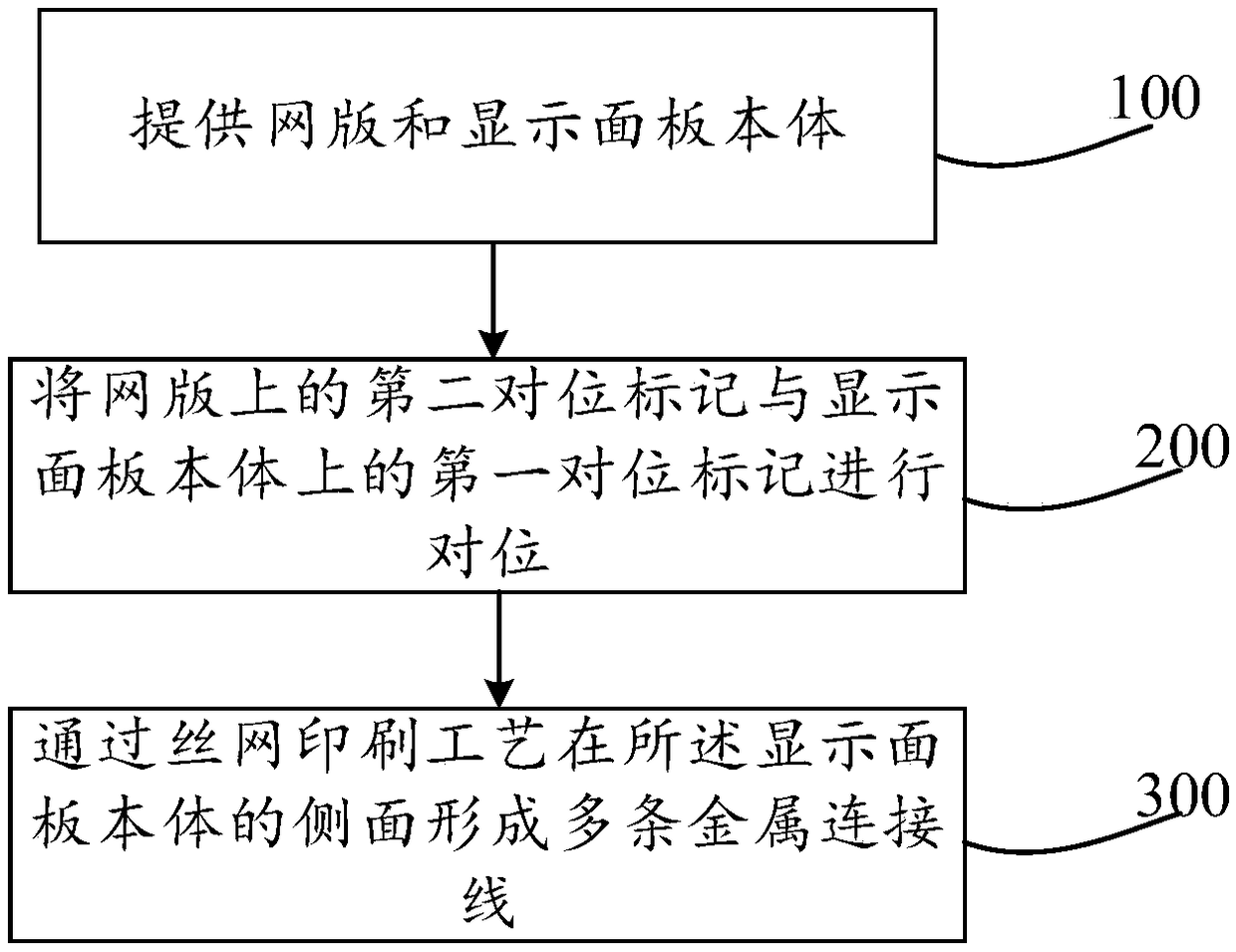
[0028] like figure 2 Shown is a flow chart of a method for manufacturing a display panel according to an embodiment of the present invention, and the method includes the following steps:
[0029] Step 100, providing a screen and a display panel body.
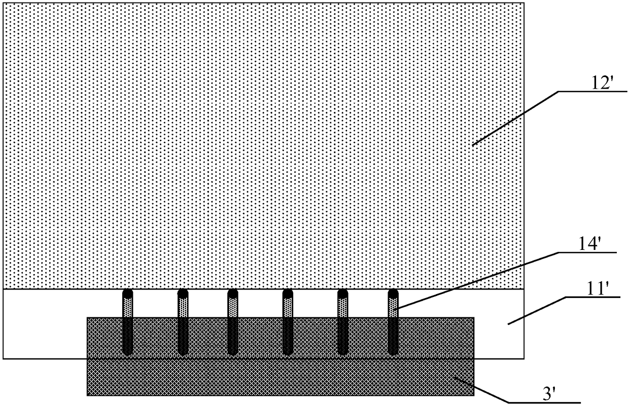
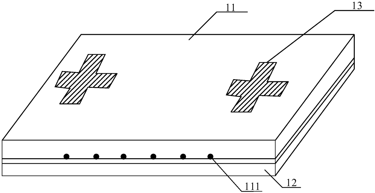
[0030] like figure 2 As shown, it is a schematic structural view of the display panel body. The display panel includes a first substrate 11 and a second substrate 12 arranged oppositely. The fir...
PUM
 Abstract
Description
Claims
Application Information
 - R&D
- Intellectual Property
- Life Sciences
- Materials
- Tech Scout
- Unparalleled Data Quality
- Higher Quality Content
- 60% Fewer Hallucinations
Browse by: Latest US Patents, China's latest patents, Technical Efficacy Thesaurus, Application Domain, Technology Topic, Popular Technical Reports.
© 2025 PatSnap. All rights reserved.Legal|Privacy policy|Modern Slavery Act Transparency Statement|Sitemap|About US| Contact US: help@patsnap.com