LED light and LED packaging method

A technology of LED packaging and LED chips, which is applied in the direction of semiconductor devices, electrical components, circuits, etc., can solve the problems of quantum efficiency reduction, affecting the lumen efficiency of LED light sources, and reducing light intensity, and achieve the effect of improving luminous dispersion

Active Publication Date: 2020-03-03
杭州般若高科技有限公司
View PDF4 Cites 0 Cited by
  • Summary
  • Abstract
  • Description
  • Claims
  • Application Information

AI Technical Summary

Problems solved by technology

[0004] LEDs that use the above method to emit light have the following defects: the distribution of light emitted by the LED light source is relatively scattered, and the illumination brightness of the light source is not good. It often needs to be shaped by an external lens to meet the brightness requirements, which greatly increases the production cost of the LED; The powder is directly coated on the surface of the chip, and the chip absorbs the scattered light, which reduces the luminous efficiency. Moreover, the high temperature of the chip will reduce the quantum efficiency of the phosphor powder, which will affect the lumen efficiency of the LED light source, which will easily lead to a decrease in light intensity. A series of problems such as spectral shift and accelerated aging of the chip reduce the service life of the LED light source

Method used


Image

  • LED light and LED packaging method
  • LED light and LED packaging method
  • LED light and LED packaging method

Examples


Embodiment 1

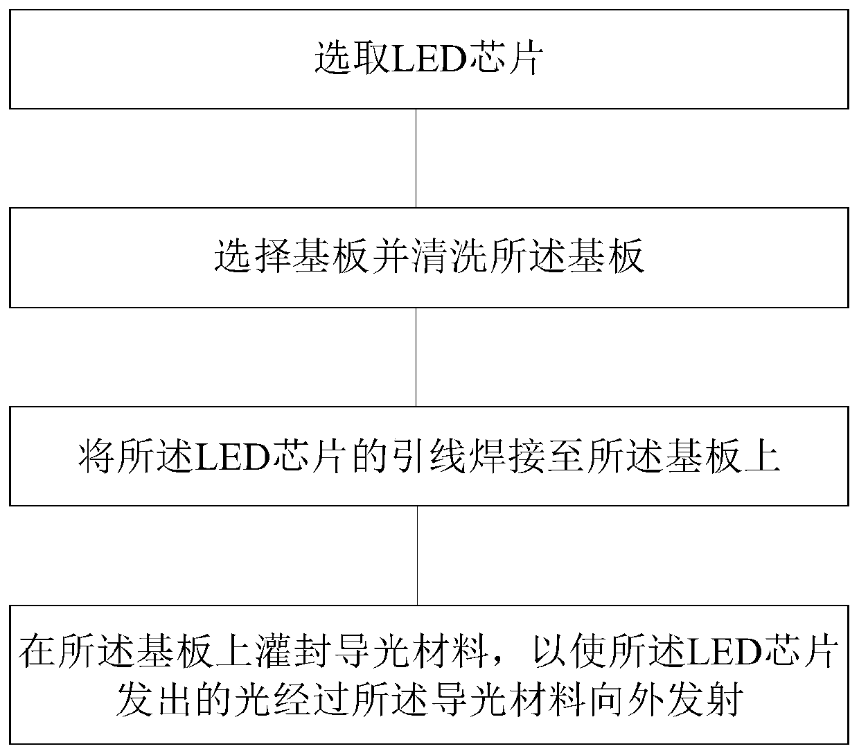
[0043] See figure 1 , figure 1 A schematic flow chart of an LED packaging method provided by an embodiment of the present invention, the method includes:

[0044] Select the LED chip;

[0045] selecting a heat sink and cleaning said heat sink;

[0046] Welding the leads of the LED chip to the heat sink;

[0047] A light guide material is potted on the heat sink, so that the light emitted by the LED chip is emitted outward through the light guide material.

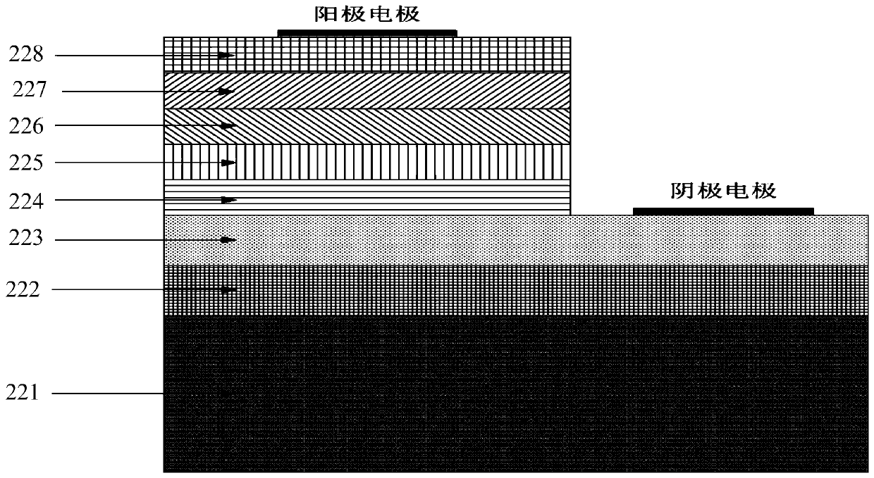
[0048] Further, on the basis of the above implementation manner, please refer to figure 2 , figure 2 A structural schematic diagram of an LED chip provided by an embodiment of the present invention, the LED chip sequentially includes a substrate layer (221), a GaN buffer layer (222), an N-type GaN layer (223), a first P-type GaN quantum well wide bandgap layer (224), InGaN layer (225), second P-type GaN quantum well wide bandgap layer (226), AlGaN barrier layer (227), P-type GaN layer (228) and electrodes.

[0049]...

Embodiment 2

[0078] This embodiment further illustrates the packaging method of the LED chip provided by the present invention.

[0079] see again image 3 ,exist image 3 In the shown heat sink, the width W of the heat sink is 0.5 mm to 10 mm, the diameter R of the circular groove is 0.2 mm to 1 mm, the distance L2 between two connected circular grooves is 0.5 mm to 10 mm, and the thickness of the heat sink is D and the length L, the distance L1 between the initial circular groove and the heat sink wall can be determined according to the process conditions, and the present invention is not limited here.

[0080] Preferably, the thickness of the heat sink used in this embodiment is relatively thick, so the heat sink will not affect the heat dissipation effect due to the reduction of the degree of fit between the heat sink and the peripheral heat dissipation device due to high temperature deformation.

[0081] please refer again Figure 4 ,exist Figure 4 Among them, the first silica ge...


PUM

PropertyMeasurementUnit
diameteraaaaaaaaaa
radiusaaaaaaaaaa
refractive indexaaaaaaaaaa

Abstract

The invention relates to an LED lamp and an LED packaging method. The packaging method comprises the steps of selecting an LED chip; selecting heat sink and cleaning the heat sink; welding a lead of the LED chip on the heat sink; and potting a light guide material on the heat sink to make light emitted from the LED chip emit outwards through the light guide material. The LED lamp provided by the invention is packaged by adopting the method; and according to the packaging method, through separation of fluorescent powder from the LED chip, the problem that the quantum efficiency and the light transmittance of the fluorescent powder are reduced due to high temperature is solved.

Description

technical field [0001] The invention belongs to the technical field of semiconductors, in particular to an LED lamp and an LED packaging method. Background technique [0002] LED (Light Emitting Diode), light-emitting diode, is a solid-state semiconductor device that can directly convert electricity into light. The practicality and commercialization of high-performance LEDs have brought about a new revolution in lighting technology. The pixel light composed of multiple ultra-high-brightness red, blue, and green LEDs can not only emit various colors of light with continuously adjustable wavelengths, but also emit white light with a brightness of tens to one hundred candlepower as a lighting source. For incandescent lamps and LED solid-state lighting lamps with the same luminance, the power consumption of the latter only accounts for 10%-20% of the former. [0003] Most of the white LEDs produced in reality are made by covering a layer of light yellow phosphor coating on the...

Claims


Application Information

Patent Timeline
Patent Type & Authority Patents(China)
IPC IPC(8): H01L33/52H01L33/56H01L33/50H01L33/58H01L33/64H01L33/62
CPCH01L33/50H01L33/52H01L33/56H01L33/58H01L33/62H01L33/641H01L33/642
Inventor 左瑜
Owner 杭州般若高科技有限公司
Why Eureka
Try Eureka