Optical scanning device

An optical scanning device and light reflection technology, applied in optics, optical components, instruments, etc., can solve the problems of narrowing the image display area and shortening the interval where the scanning speed of the optical scanning device is constant, and achieve the effect of suppressing transients

Active Publication Date: 2022-02-25
MITSUMI ELECTRIC CO LTD
View PDF19 Cites 0 Cited by
  • Summary
  • Abstract
  • Description
  • Claims
  • Application Information

AI Technical Summary

Problems solved by technology

However, if a plurality of filters are used, the linearity of the voltage applied to the driving source decreases, and the interval in which the scanning speed of the optical scanning device is constant becomes shorter.
Therefore, the area available for image display is narrowed

Method used


Image

  • Optical scanning device
  • Optical scanning device
  • Optical scanning device

Examples


no. 1 approach

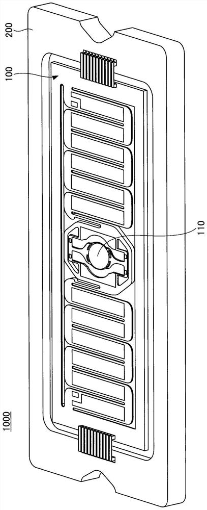
[0028] First, the optical scanning device according to the first embodiment will be described. figure 1 as well as figure 2 is a perspective view showing an example of the optical scanning device according to the first embodiment, figure 1 An optical scanning device showing a state in which the encapsulation cover is removed, figure 2 It shows the optical scanning device in the state where the package cover is attached.

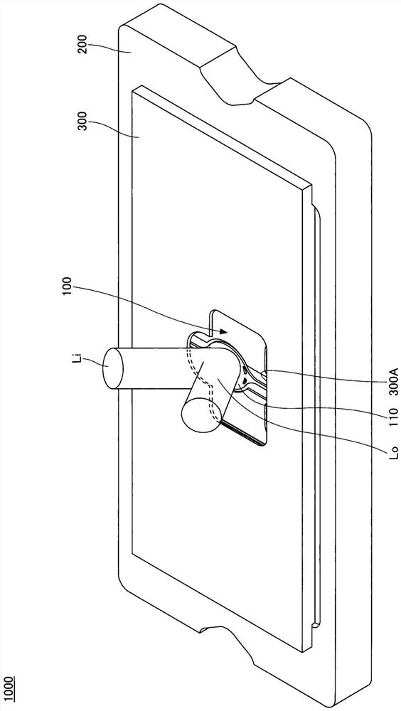
[0029] Such as figure 1 as well as figure 2 As shown, the optical scanning device 1000 includes an optical scanning unit 100 , a ceramic package 200 on which the optical scanning unit 100 is mounted, and a package cover 300 disposed on the ceramic package 200 and covering the optical scanning unit 100 . The optical scanning device 1000 may include a substrate, a control circuit, and the like on the lower side of the ceramic package 200 .

[0030] In the optical scanning device 1000 , an opening 300A that exposes the vicinity of the reflective mirror 1...

no. 2 approach

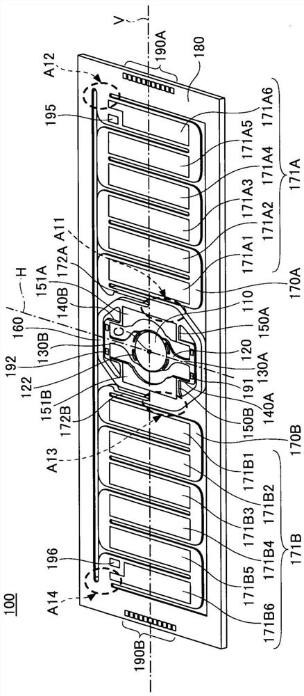
[0065] An optical scanning device according to a second embodiment will be described. Figure 11 It is a perspective view showing an example of the optical scanning device of the second embodiment on the upper side. Figure 12 It is a perspective view showing the bottom side of an example of the optical scanning unit of the optical scanning device according to the second embodiment.

[0066] Such as Figure 11 and Figure 12 As shown, the optical scanning unit 100A of the second embodiment is the same as the first one in that the second drive beam 170A and the second drive beam 170B have a point-symmetrical arrangement relationship with the center C of the light reflection surface of the mirror 110 as a point of symmetry. The optical scanning unit 100 of the embodiment is different. In addition, other configurations can be the same as those of the optical scanning unit 100 of the first embodiment.

[0067] In the optical scanning unit 100A of the second embodiment, the mov...


PUM


Abstract

The present invention provides an optical scanning device capable of securing an area for image display and suppressing generation of transients. An optical scanning device according to one embodiment includes a reflector having a light reflecting surface, a movable frame supporting the reflector, a pair of driving beams supporting the movable frame from both sides, and a pair of driving beams provided on the driving beam so that the movable frame A driving source that swings around a predetermined axis, a fixed frame supporting the above-mentioned driving beam, and a movable frame connecting portion connecting the above-mentioned movable frame and the above-mentioned driving beam are arranged and arranged to connect the above-mentioned fixed frame and the above-mentioned driving beam with respect to the above-mentioned predetermined axis. The side of the fixed frame connection portion is roughly the opposite side.

Description

technical field [0001] The present invention relates to optical scanning devices. Background technique [0002] Conventionally, an optical scanning device is known that includes a movable plate having a light-reflecting surface that reflects incident light, a torsion beam that rotatably supports the movable plate, and a drive source that acts on the torsion beam in a twisting direction. [0003] When such an optical scanning device is used in an image display device, if the scanning speed is not constant, the image will be skewed in the scanning direction. Therefore, an area where the scanning speed is constant is used for image display. In order to keep the scanning speed constant, it is required to be able to apply a highly linear voltage, that is, a voltage with a long linear section in one cycle, to the drive source. [0004] Therefore, conventionally, by applying a saw-tooth waveform voltage to a driving source, the interval in which the scanning speed of the optical ...

Claims


Application Information

Patent Timeline
Patent Type & Authority Patents(China)
IPC IPC(8): G02B26/10G02B26/08
CPCG02B26/0858G02B26/105G02B26/101H10N30/2044
Inventor 山田司
Owner MITSUMI ELECTRIC CO LTD
Why Eureka
Try Eureka