
Display module and display device

A display module and display area technology, applied in instruments, nonlinear optics, optics, etc., can solve problems such as the inability to meet the thinning trend of the display screen, the overall thickness of the display screen becomes larger, and the display screen is prone to color shift, etc. Meet the thinning trend, reduce thickness, and reduce the effect of height difference

Inactive Publication Date: 2018-03-16
WUHAN TIANMA MICRO ELECTRONICS CO LTD
View PDF9 Cites 41 Cited by
  • Summary
  • Abstract
  • Description
  • Claims
  • Application Information

AI Technical Summary

Problems solved by technology

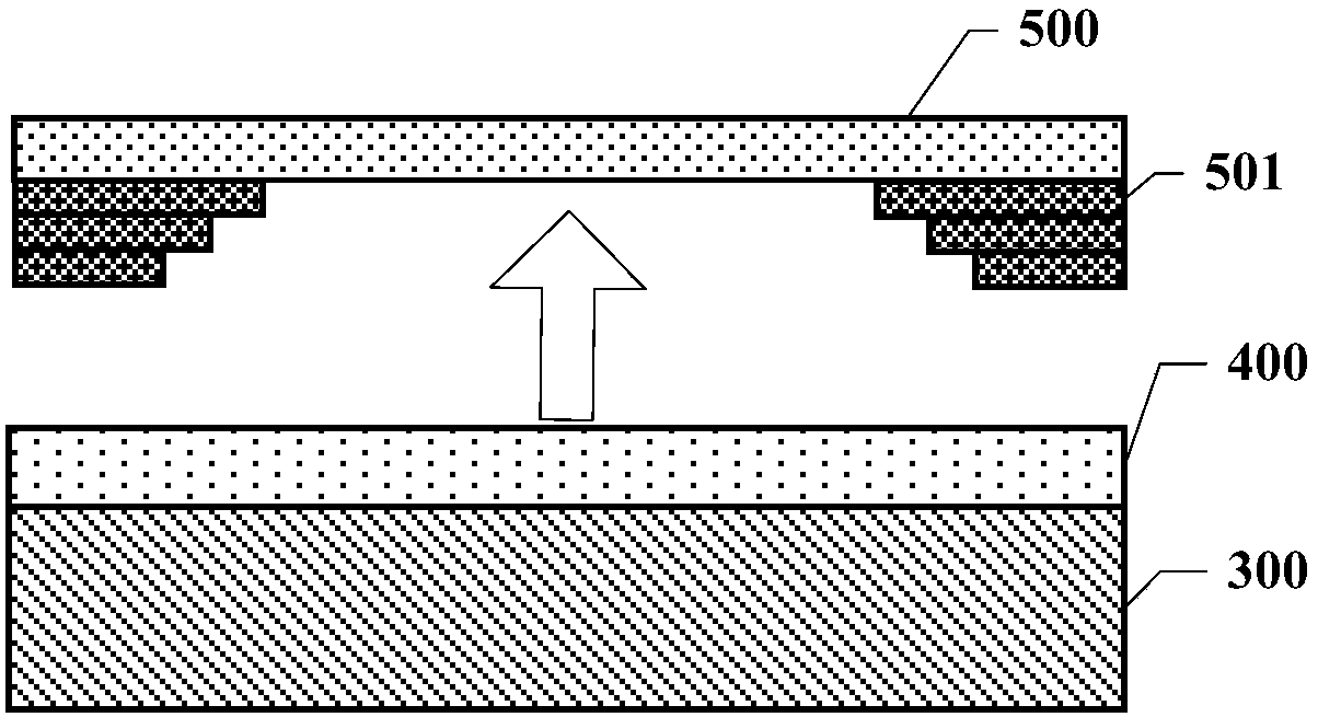
The total thickness of the multi-layer ink layer is relatively large, and the height difference between the ink layer and the substrate is relatively large. If the thickness of the optical glue used is thin, it is easy to generate adhesion bubbles during the process of attaching the substrate and cover plate, and It is very easy to produce color shift after the display is turned on. If the thickness of the optical glue used is large, the cost of the optical glue will be increased, and the overall thickness of the display will become larger, which cannot meet the requirements of the thinning trend of the display.

Method used


Image

  • Display module and display device
  • Display module and display device
  • Display module and display device

Examples


Embodiment Construction

[0026] Certain terms are used, for example, in the description and claims to refer to particular components. Those skilled in the art should understand that hardware manufacturers may use different terms to refer to the same component. The specification and claims do not use the difference in name as a way to distinguish components, but use the difference in function of components as a criterion for distinguishing. As mentioned throughout the specification and claims, "comprising" is an open term, so it should be interpreted as "including but not limited to". "Approximately" means that within an acceptable error range, those skilled in the art can solve the technical problem within a certain error range and basically achieve the technical effect. In addition, the term "coupled" herein includes any direct and indirect electrical coupling means. Therefore, if it is described that a first device is coupled to a second device, it means that the first device may be directly elect...


PUM

PropertyMeasurementUnit
thicknessaaaaaaaaaa
thicknessaaaaaaaaaa
thicknessaaaaaaaaaa

Abstract

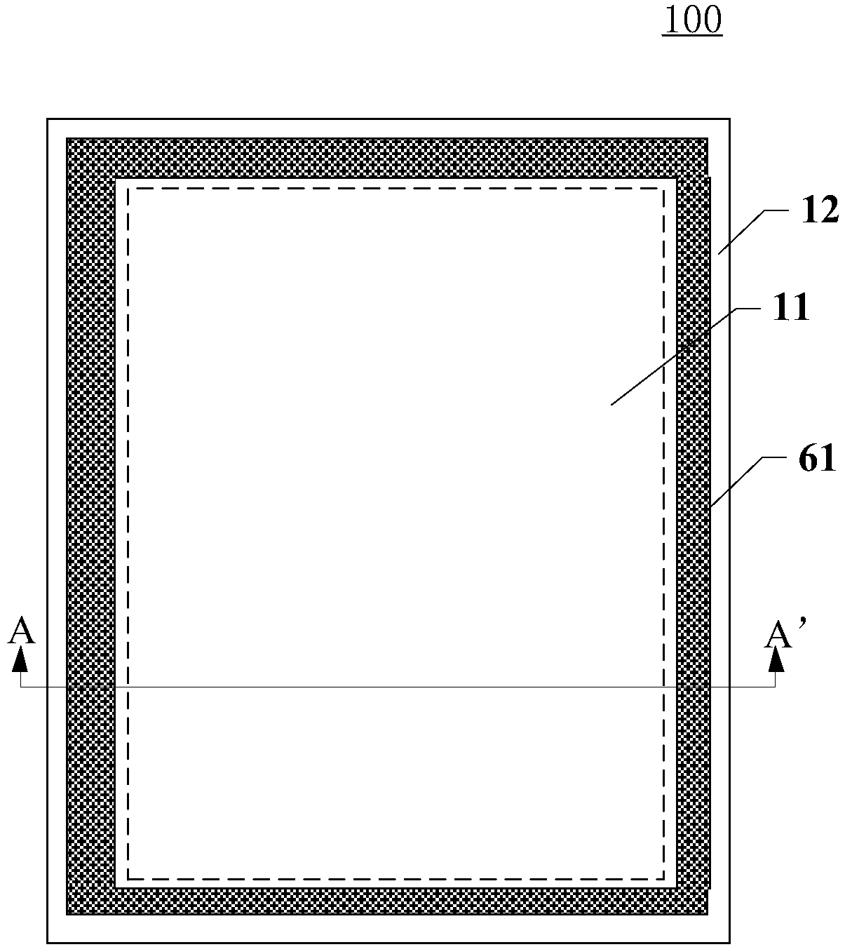
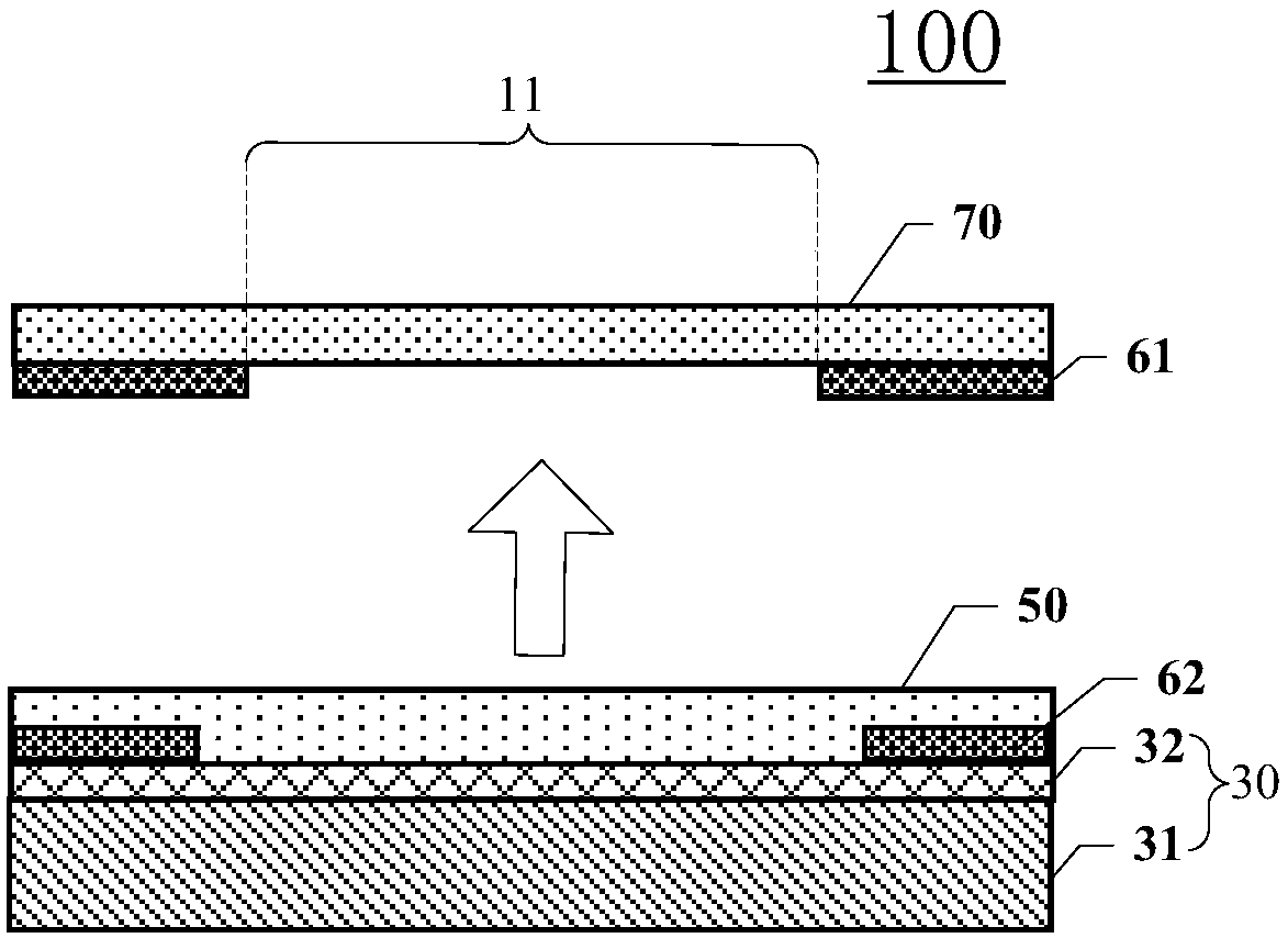
The invention discloses a display module and a display device, and relates to the technical field of display. The display module is provided with a display area and a non-display area arranged aroundthe display area, the display module comprises a display panel and a cover plate, and the display panel and the cover plate are attached through optical glue; the display panel comprises an array substrate and a polarizer which are sequentially arranged, and the polarizer is located on the side, close to the cover plate, of the array substrate; the display module comprises at least two layers of ink layers, and the ink layers are located in the non-display area and surround the display area; the at least two layers of ink layers comprise the first ink layer and at least one second ink layer, the first ink layer is arranged on the surface, close to one side of the display panel, of the cover plate, and at least one second ink layer is arranged between the optical glue and the array substrate. Therefore, the height difference between the ink layer on the cover plate and the display panel is effectively reduced so that the phenomena that bubbles are generated in the attaching process andcolor cast is generated in the display process can be avoided, and the requirement for the thinning tendency of the display module and the display device can be met.

Description

technical field [0001] The present application relates to the field of display technology, in particular, to a display module and a display device. Background technique [0002] In recent years, liquid crystal display devices or organic electroluminescence display devices, as the mainstream products in flat panel display technology, have a wide range of applications, ranging from small consumer products such as mobile phones and digital cameras to desktop computer display areas, televisions, head-up displays, etc. Large displays are applied to every aspect of people's lives. [0003] Before leaving the factory, the substrate with the display function in the display device usually needs to be attached to the cover with optical glue. Usually, in order to prevent light leakage in the display device, during the production of the cover, the non-display Set 2 to 4 layers of light-shielding ink layers in the area, and then attach the substrate and the side of the cover plate on wh...

Claims


Application Information

Patent Timeline
Patent Type & Authority Applications(China)
IPC IPC(8): G02F1/1333G02F1/1335
CPCG02F1/133308G02F1/133528G02F1/133331
Inventor 占栋
Owner WUHAN TIANMA MICRO ELECTRONICS CO LTD
Learn More