Touch screen of electronic device and electronic device
A technology of electronic equipment and touch screen, which is applied in the direction of electrical digital data processing, input/output process of data processing, instruments, etc., can solve problems such as unfavorable cost saving, waste materials, etc., and achieve the effect of saving material cost and reducing area
- Summary
- Abstract
- Description
- Claims
- Application Information
AI Technical Summary
Problems solved by technology
Method used
Image
Examples
Embodiment 1
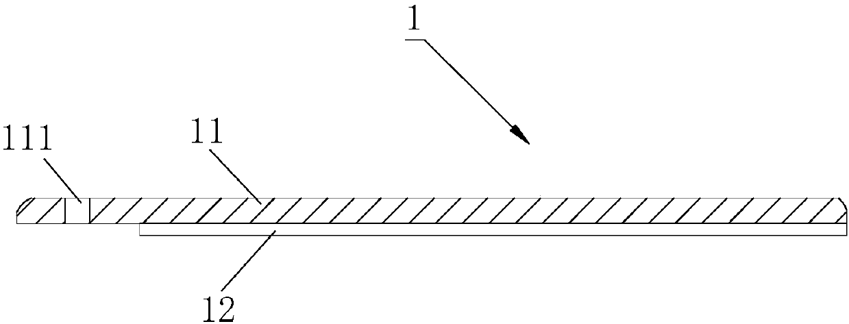
[0030] See figure 1 , a touch screen 1 of an electronic device provided in this embodiment, including a cover plate 11 and a sensing film 12, the cover plate 11 and the sensing film 12 are stacked together, and the area of the sensing film 12 is smaller than the area of the cover plate 11, Moreover, the position of the sensing film 12 is offset from one end of the cover plate 11 . One end of the cover plate 11 is provided with a sound outlet 111 for the electronic device to emit sound, and the position of the sensing film 12 is staggered from the sound outlet 111 .
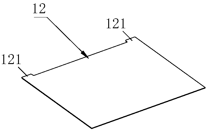
[0031] See also figure 2 A connection portion 121 for connecting with the middle frame of the electronic device extends from a part of the end of the sensing film 12 . One end of the sensing film 12 near the sound outlet 111 forms a step with the cover 11 , and the peripheral edge of the sensing film 12 also forms a step with the cover 11 .
[0032] Because some electronic devices, such as mobile phones, t...
Embodiment 2
[0042] See Figure 8 , this embodiment provides another electronic device 100', including a touch screen 1' and a middle frame 2', and the touch screen 1' includes a cover plate 11' and a sensing film 12'. The difference from the first embodiment is that this embodiment The touch screen 1' of the example also includes a common thin film 13' which only plays a filling role. Since the ordinary film 13' has no induction effect, the total production cost is much lower than that of the induction film 12', and the ordinary film 13' is bonded with the cover plate 11' by a glue layer 14'.
[0043] A first connecting portion 21' and a second connecting portion 22' are disposed inside the middle frame 2'. The cover plate 11' is bonded to the top surface of the ordinary film 13' through the glue layer 14 in the area where the sensing film 12' is staggered, and the bottom surface of the ordinary film 13' is connected to the first one through another glue layer 3. part 21', and the edge ...
PUM
 Abstract
Description
Claims
Application Information
 - R&D
- Intellectual Property
- Life Sciences
- Materials
- Tech Scout
- Unparalleled Data Quality
- Higher Quality Content
- 60% Fewer Hallucinations
Browse by: Latest US Patents, China's latest patents, Technical Efficacy Thesaurus, Application Domain, Technology Topic, Popular Technical Reports.
© 2025 PatSnap. All rights reserved.Legal|Privacy policy|Modern Slavery Act Transparency Statement|Sitemap|About US| Contact US: help@patsnap.com


