Pixel structure
A pixel structure, pixel electrode technology, applied in nonlinear optics, instruments, optics, etc., can solve the problems of color shift and viewing angle, achieve wide viewing angle display effect, improve display aperture ratio, improve color shift phenomenon and viewing angle problems. Effect
- Summary
- Abstract
- Description
- Claims
- Application Information
AI Technical Summary
Problems solved by technology
Method used
Image
Examples
Embodiment Construction
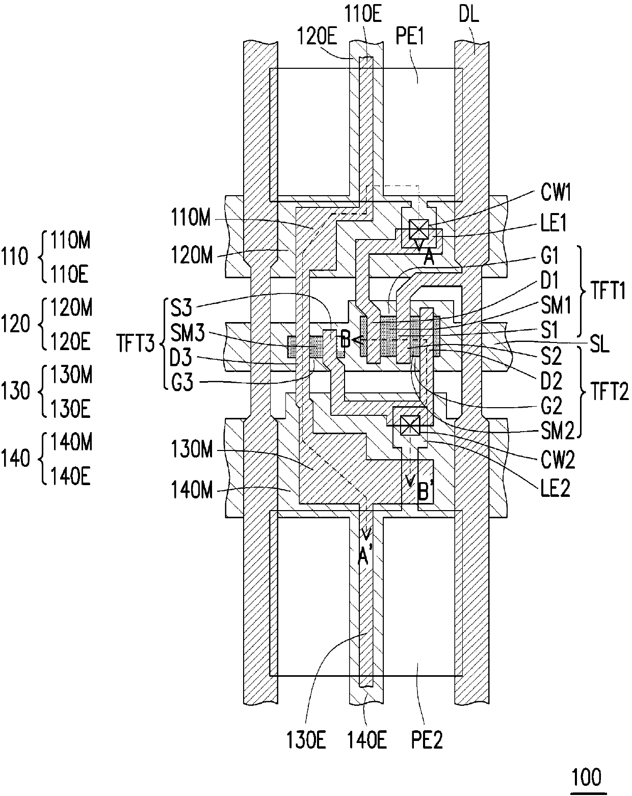
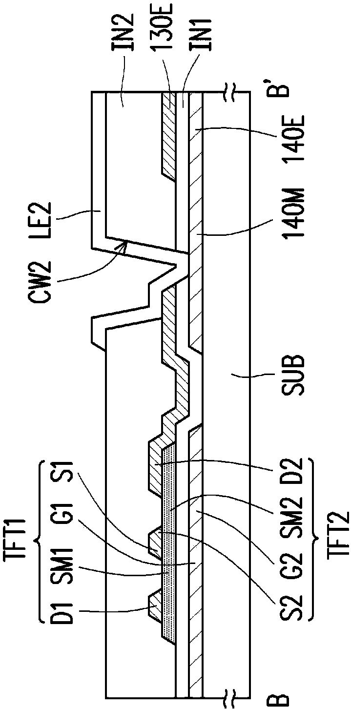
[0061] figure 1 It is a schematic top view of a pixel structure according to an embodiment of the present invention. figure 2 yes figure 1 The schematic cross-sectional view of the pixel structure along the section line A-A'. image 3 yes figure 1 The schematic cross-sectional view of the pixel structure along the section line B-B'. For clarity and ease of explanation, figure 1 Partial film layers are omitted. Below, will pass Figure 1 to Figure 3 An embodiment of the present invention will be described in detail.
[0062] The pixel structure 100 includes a first active element TFT1, a first pixel electrode PE1, a first capacitor electrode 110, a second capacitor electrode 120, a second active element TFT2, a second pixel electrode PE2, a third capacitor electrode 130, and a fourth capacitor electrode 140 and the third active element TFT3. In some embodiments, the pixel structure 100 further includes a scan line SL, a data line DL, a first insulating layer IN1, a sec...
PUM
 Abstract
Description
Claims
Application Information
 - R&D
- Intellectual Property
- Life Sciences
- Materials
- Tech Scout
- Unparalleled Data Quality
- Higher Quality Content
- 60% Fewer Hallucinations
Browse by: Latest US Patents, China's latest patents, Technical Efficacy Thesaurus, Application Domain, Technology Topic, Popular Technical Reports.
© 2025 PatSnap. All rights reserved.Legal|Privacy policy|Modern Slavery Act Transparency Statement|Sitemap|About US| Contact US: help@patsnap.com


