
Specific n and p active materials for organic photoelectric conversion layers in organic photodiodes

A technology of N-R2 and naphthalene diimide, applied in photovoltaic power generation, organic chemistry, circuits, etc., can solve the problems of spatial resolution, light collection and utilization efficiency reduction

Active Publication Date: 2018-01-05
SONY GRP CORP
View PDF5 Cites 4 Cited by
  • Summary
  • Abstract
  • Description
  • Claims
  • Application Information

AI Technical Summary

Problems solved by technology

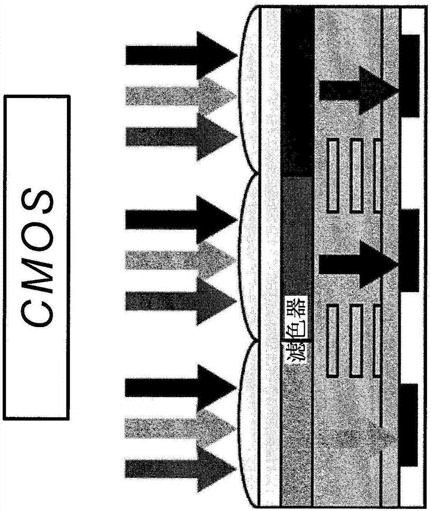
In this case, as well as in the case of color filters, the light is separated according to the color, but the spatial resolution and light collection amount and utilization efficiency are reduced

Method used


Image

  • Specific n and p active materials for organic photoelectric conversion layers in organic photodiodes
  • Specific n and p active materials for organic photoelectric conversion layers in organic photodiodes
  • Specific n and p active materials for organic photoelectric conversion layers in organic photodiodes

Examples


Embodiment 1

[0414] Example 1: Naphthalene diimide (NDI) based materials

[0415] Naphthalene diimide (NDI) NDI1 has the following chemical structure:

[0416]

[0417] exist Figure 5 In the schemes shown, general synthetic routes for the synthesis of the materials are reported.

[0418] via HPLC, 1 Material NDI1 was characterized by H NMR, mass spectrometry, TG and DSC. Figure 6 to Figure 9 The data are shown in .

[0419] The absorption spectrum shows a very low optical density in the visible range ( Figure 10 ). Electron mobility up to 10 -7 up to 10 -5 cm 2 / Vs( Figure 11 ).

[0420]NDI1 was used as acceptor material in combination with quinacridone (QD) and tributylquinacridone (BQD) as donors for the following constructs:

[0421] ITO / 8nm HG01 / 120nm QD&NDI1(1:1) / 3,5nmNBPhen / 100nm AlSiCu / 100nm LiF

[0422] ITO / 5nm MoO3 / 8nm HG01 / 120nm QD&NDI1(1:1) / 3,5nmNBPhen / 100nm AlSiCu / 100nm LiF

[0423] ITO / 8nm HG01 / 120nm BQD&NDI1(7:3) / 3,5nmNBPhen / 100nm AlSiCu / 100nm LiF

[0424...

Embodiment 2

[0430] Example 2: Further naphthalene diimide (NDI) based materials

[0431] Naphthalimides (NDI) NDI20-26, NDI 28-29 and NDI35-38 have the following chemical structures:

[0432]

[0433]

[0434] exist Figure 15 In the schemes shown, general synthetic routes for the synthesis of the materials are reported.

[0435] NDI materials show absorption maxima in the range of 379 to 385 nm ( Figure 16 ).

[0436] Figure 17 to Figure 1 The energy levels are shown in 9.

[0437] NDI35 was used as n-buffer material in devices of DTT2, DTT9, DTT10 or DTT11 respectively with F6SubPcOC6F5 in the following configuration:

[0438] LiF 150nm / AlSiCu 100nm / NDI35 10nm / DTT9:F6SubPcOC6F5(1:1) 200nm / ST116310nm / ITO / Glass.

[0439] The device is characterized, for example, by measuring the action spectrum at 0V and -1V. The results are shown in FIGS. 20 and 21 .


PUM


Abstract

The field of the DISCLOSURE lies in active materials for organic image sensors. The present disclosure relates to naphtalene diimide-based molecules and naphtalene diimide dimer-based molecules. The present disclosure relates to transparent N materials and / or to transparent P materials including the molecule(s) according to the present disclosure and their use in absorption layer(s), photoelectricconversion layer(s) and / or an organic image sensor and methods for their synthesis. The present disclosure also relates to photoelectric conversion layer(s) including an active material according tothe present disclosure, to a device, including active material(s) according to the present disclosure or photoelectric conversion layer(s) according to the present disclosure. Moreover, the present disclosure relates to an organic image sensor including photoelectric conversion layer(s) according to the present disclosure.

Description

technical field [0001] The field of the disclosure is active materials for organic image sensors. [0002] The present disclosure relates to naphthalimide-based molecules and naphthalimide dimer-based molecules. [0003] The present disclosure relates to transparent N materials and / or transparent P materials comprising molecules according to the present disclosure and their use in absorbing layers, photoelectric conversion layers and / or organic image sensors and methods for their synthesis. [0004] The present disclosure also relates to a photoelectric conversion layer comprising the active material according to the present disclosure, a device comprising the active material according to the present disclosure, or a photoelectric conversion layer according to the present disclosure. [0005] Also, the present disclosure relates to an organic image sensor including the photoelectric conversion layer according to the present disclosure. Background technique [0006] The "Ba...

Claims


Application Information

Patent Timeline
Patent Type & Authority Applications(China)
IPC IPC(8): C07D471/06H01L51/46H01L51/42
CPCY02E10/549C07D471/06Y02P70/50H10K39/32H10K85/621H10K85/654H10K30/211H10K30/30H10K85/657H10K19/20H10K85/649H10K85/6572
Inventor 西尔维娅·罗塞利特森卡·米特瓦维托尔·戴希曼大卫·丹纳威廉·福德丹尼斯·彻尔卡弗拉基米尔·雅库特金拉尔斯·彼得·舍勒尼古劳斯·克诺尔加布里埃莱·内尔斯
Owner SONY GRP CORP
Learn More