Electric power communication optical path alternate routing analysis method and device
An analysis method and detour technology, which is applied in the field of power communication optical circuit detour analysis, can solve the problems of high labor cost and complicated detour analysis operation, and achieve the effect of reducing labor cost, saving time and energy, and strong practicability
- Summary
- Abstract
- Description
- Claims
- Application Information
AI Technical Summary
Problems solved by technology
Method used
Image
Examples
Embodiment 1
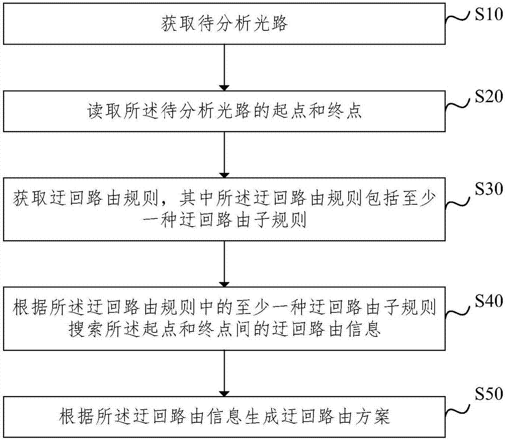
[0051] figure 1 It is a schematic diagram of the method for analyzing the circuitous circuit of a communication optical path according to an embodiment of the present invention, such as figure 1 As shown, the embodiment of the present invention provides a method for analyzing the circuitous circuit of a communication optical path, including:
[0052] Step S10: Obtain the optical path to be analyzed;
[0053] Step S20: Read the start point and end point of the light path to be analyzed;
[0054] Step S30: Obtain a detour route rule, where the detour route rule includes at least one detour route sub-rule;
[0055] Step S40, searching for the detour information between the start and end points according to at least one detour sub-rule in the detour rules;
[0056] Step S50: Generate a detour plan based on the detour route information.
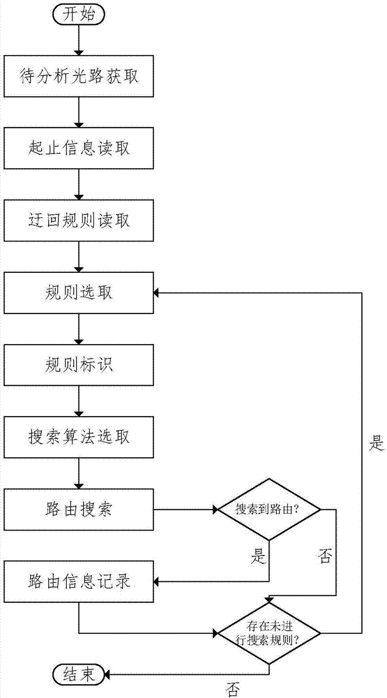
[0057] Specifically, a method for analyzing the detour route of power communication optical path includes three links: detour route analysis and summary, de...
Embodiment 2
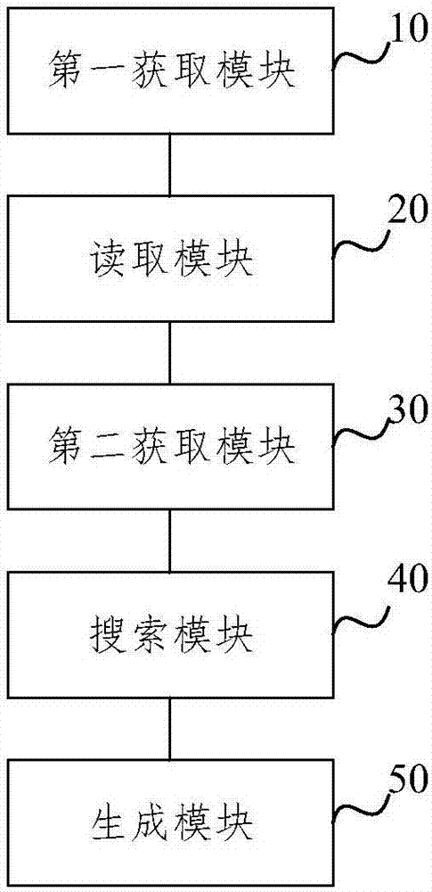
[0137] image 3 It is a schematic diagram of a communication optical path circuit analysis device according to an embodiment of the present invention, such as image 3 As shown, the embodiment of the present invention provides a communication optical path circuit analysis device, including a first acquisition module 10, a reading module 20, a second acquisition module 30, a search module 40, and a generation module 50, wherein:
[0138] The first obtaining module 10 is used to obtain the optical path to be analyzed;
[0139] The reading module 20 is used to read the start and end points of the optical path to be analyzed;
[0140] The second obtaining module 30 is configured to obtain a detour route rule, wherein the detour route rule includes at least one detour route sub-rule;
[0141] The search module 40 is configured to search for the detour information between the starting point and the end point according to at least one detour sub-rule in the detour rules;
[0142] The generatin...
Embodiment 3
[0150] Figure 4 It is a schematic structural diagram of an electronic device for analyzing the circuitous circuit of a communication optical path provided by an embodiment of the present invention, such as Figure 4 As shown, the device includes: a processor (processor) 801, a memory (memory) 802 and a bus 803;
[0151] Wherein, the processor 801 and the memory 802 communicate with each other through the bus 803;
[0152] The processor 801 is configured to call program instructions in the memory 802 to execute the methods provided in the foregoing method embodiments, for example, including: obtaining the optical path to be analyzed;
[0153] Reading the start and end points of the light path to be analyzed;
[0154] Obtaining a detour route rule, wherein the detour route rule includes at least one detour route sub-rule;
[0155] Searching for the detour route information between the start point and the end point according to at least one detour route sub-rule in the detour route rule...
PUM
 Abstract
Description
Claims
Application Information
 - R&D
- Intellectual Property
- Life Sciences
- Materials
- Tech Scout
- Unparalleled Data Quality
- Higher Quality Content
- 60% Fewer Hallucinations
Browse by: Latest US Patents, China's latest patents, Technical Efficacy Thesaurus, Application Domain, Technology Topic, Popular Technical Reports.
© 2025 PatSnap. All rights reserved.Legal|Privacy policy|Modern Slavery Act Transparency Statement|Sitemap|About US| Contact US: help@patsnap.com


